
NVIDIA has transitioned from a niche graphics card manufacturer to the most pivotal player in the global technology landscape. As the architect of the modern Artificial Intelligence (AI) revolution, the company’s physical presence is as much a statement of its engineering prowess as the chips it produces. For those looking to understand where the future of computing is being written, the answer lies at 2788 San Tomas Expressway, Santa Clara, California.
NVIDIA’s global headquarters is not merely a collection of office buildings; it is a high-tech ecosystem designed to foster the next generation of accelerated computing. Spanning across a massive campus in the heart of Silicon Valley, the site serves as the nerve center for the hardware and software breakthroughs that power everything from ChatGPT to autonomous vehicles.
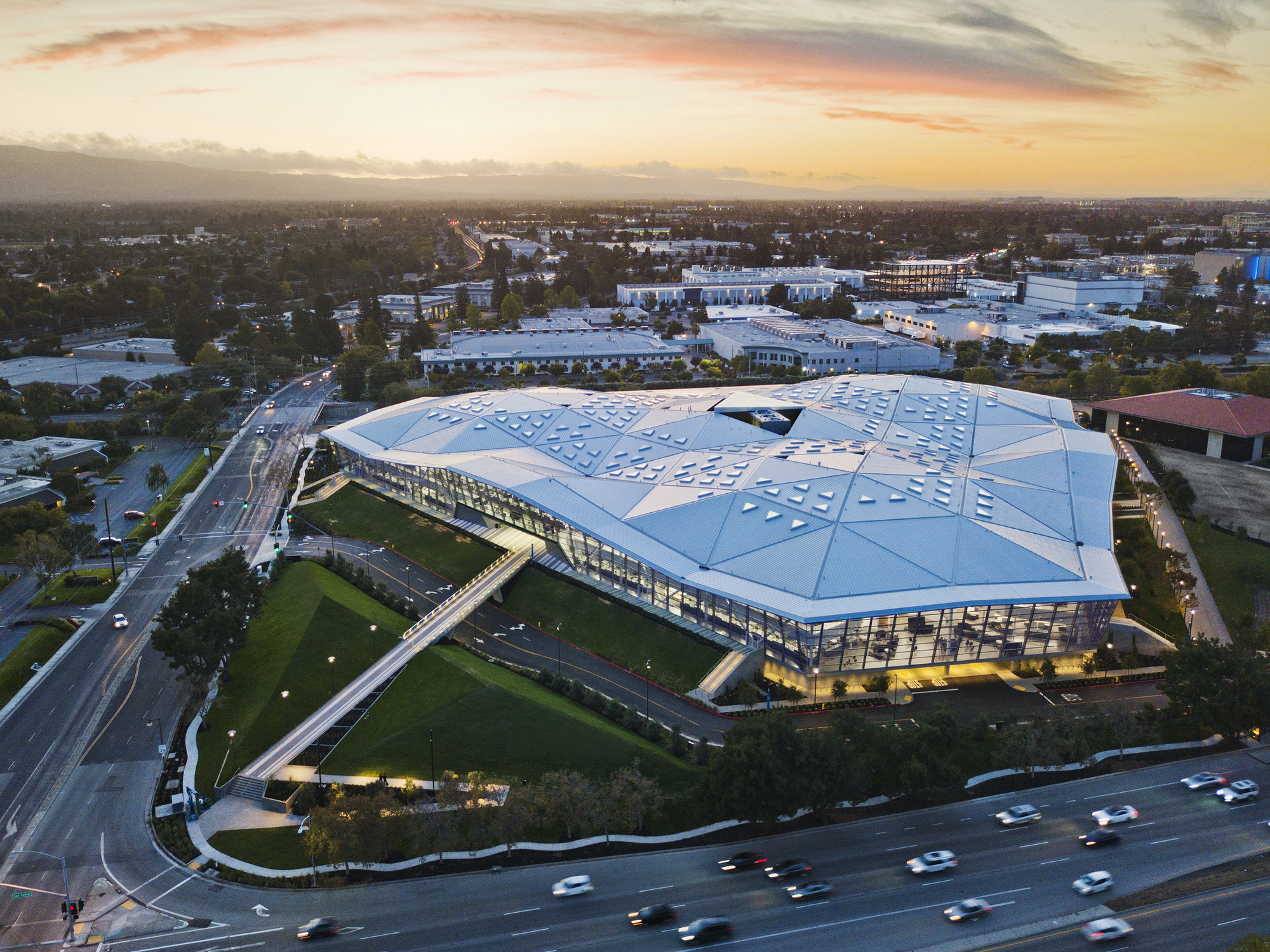
Santa Clara: The Epicenter of the GPU Revolution
The choice of Santa Clara as the site for NVIDIA’s headquarters is deeply symbolic of the company’s history and the broader evolution of the semiconductor industry. Situated in the South Bay region of the San Francisco Bay Area, Santa Clara is the historic ground zero for the “Silicon” in Silicon Valley. By anchoring itself here, NVIDIA remains at the crossroads of talent, research institutions, and fellow tech titans.
Architectural Innovation: Endeavor and Voyager
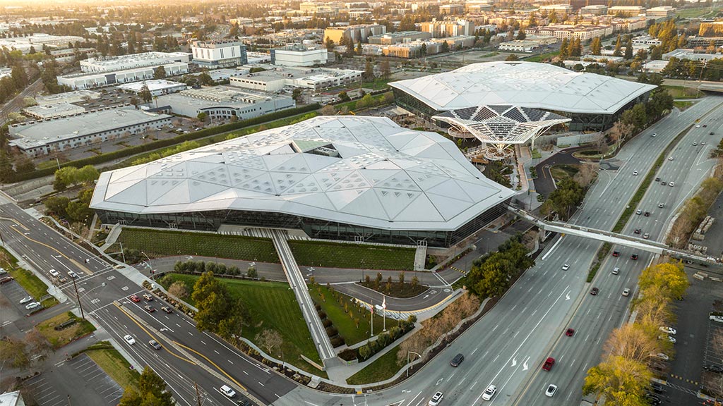
The NVIDIA campus is defined by two flagship structures: “Endeavor” and “Voyager.” These names are not accidental; they reflect the company’s mission to push the boundaries of what is technologically possible. Endeavor, the first of the two, opened in 2017 and spans 500,000 square feet. Its successor, Voyager, added another 750,000 square feet to the campus footprint when it opened in 2022.
Architecturally, these buildings are an homage to the fundamental building block of computer graphics: the triangle. From the skylights to the floor plans, the triangular geometry represents the “polygons” used to render 3D images—the technology that originally put NVIDIA on the map. The structures are designed with massive open floor plans, intended to break down the silos often found in legacy tech firms.
A Design for Collaboration and Fluidity
In the world of high-tech engineering, breakthroughs rarely happen in isolation. NVIDIA’s headquarters is meticulously engineered to encourage “collision” between different departments. The interior layout uses a “non-hierarchical” design, where executives and junior engineers work in proximity.
The vertical movement within the buildings is handled by grand staircases and ramps rather than hidden elevators, ensuring that employees from the hardware divisions frequently interact with those from the software and AI research teams. This fluidity is essential for NVIDIA’s full-stack approach, where software (like the CUDA platform) must be perfectly synchronized with hardware (the H100 and Blackwell GPUs).
Inside the AI Foundry: How the Campus Drives Innovation
While many tech headquarters focus on aesthetic luxury, NVIDIA’s Santa Clara base is a functional “AI foundry.” It houses some of the most advanced laboratories in the world, where the next generation of Hopper and Blackwell architectures are simulated, tested, and refined before they ever reach a fabrication plant.
Specialized Labs and Hardware Stress Testing
Beneath the sleek glass and metal exterior of the headquarters lies a labyrinth of high-performance computing (HPC) labs. These facilities are dedicated to thermal management testing, electromagnetic interference (EMI) shielding, and signal integrity. As GPUs become more powerful, they generate immense heat and consume significant power. The engineering teams in Santa Clara work around the clock to solve the physics-defying challenges of packing billions of transistors into a single die.
The campus also features specialized robotics labs. Here, NVIDIA’s “Isaac” platform is developed, allowing researchers to test AI models in both physical and simulated environments. Using “digital twins”—virtual replicas of the physical world—engineers can train autonomous machines in a digital space before deploying the code into physical robots on the campus floor.
The Nexus of CUDA and Software Development
NVIDIA is as much a software company as it is a hardware company. The Santa Clara headquarters serves as the primary hub for the development of CUDA (Compute Device Unified Architecture), the parallel computing platform that transformed the GPU from a gaming component into a general-purpose processor for science and AI.
Thousands of software engineers at the headquarters work on optimizing libraries for deep learning, large language models (LLMs), and real-time ray tracing. The proximity of these software teams to the hardware designers allows for a feedback loop that is unique in the industry. When a software engineer identifies a bottleneck in how an AI model processes data, they can walk across the “Endeavor” floor to discuss a hardware-level fix with a silicon architect.
A Headquarters Built on Sustainable Tech and Smart Infrastructure
As a leader in technology, NVIDIA recognizes that the massive energy requirements of AI must be balanced with sustainable practices. The headquarters itself serves as a pilot program for how large-scale tech campuses can operate with a minimal carbon footprint.
Sustainable Energy and Water Integration
The “Voyager” building is a marvel of green engineering. It is designed to be a LEED Gold-certified structure, utilizing a variety of “smart” environmental controls. One of the most striking features is the trellis system on the roof, which is covered in solar panels. These panels do more than just generate electricity; they provide shade, reducing the energy needed to cool the building during the intense California summers.
Furthermore, the campus utilizes a sophisticated reclaimed water system. In a region frequently hit by droughts, NVIDIA’s headquarters uses recycled water for its cooling towers and landscaping. This creates a closed-loop system that demonstrates how high-density computing hubs can coexist with local environmental constraints.
Smart Building Management Systems
The headquarters is essentially a “living computer.” Thousands of sensors are embedded throughout the campus to monitor everything from occupancy levels to air quality and light intensity. This data is fed into a centralized management system—likely powered by NVIDIA’s own AI—to optimize energy consumption in real-time.
For example, the lighting system uses “daylight harvesting,” where sensors measure the amount of natural light entering through the triangular skylights and adjust the LED brightness accordingly. This tech-first approach to facility management reduces overhead and serves as a blueprint for the “smart cities” NVIDIA’s technology aims to build globally.
From Santa Clara to the World: Scaling the AI Ecosystem
The influence of the Santa Clara headquarters extends far beyond the borders of California. It serves as the “brain” of a global network of R&D centers, data centers, and partner ecosystems. The decisions made at 2788 San Tomas Expressway dictate the technological roadmap for the entire planet.
Supporting the Global Data Center Network
While the chips are designed in Santa Clara, they are deployed in massive data centers around the world. The headquarters acts as the central command for the NVIDIA DGX Cloud, a service that allows enterprises to access AI supercomputing power via the web. The engineers at the headquarters monitor the performance of these global clusters, using the data to inform the design of future silicon.
The campus also serves as a training ground for the global developer community. NVIDIA frequently hosts technical workshops and “hackathons” at its headquarters, inviting the brightest minds in tech to learn how to harness the power of accelerated computing. This creates a virtuous cycle where the tools developed in Santa Clara become the industry standard worldwide.

The Future of the Silicon Valley Tech Hub
In an era where remote work has become common, NVIDIA has doubled down on the importance of a physical headquarters. By creating a space that is more than just an office—a space that is an engineering tool in its own right—NVIDIA has ensured that Santa Clara remains the focal point of the AI era.
As NVIDIA continues to expand, the headquarters will likely see further evolution. With the rise of generative AI and the increasing demand for specialized “AI Factories,” the Santa Clara campus will continue to serve as the prototype for the infrastructure of the future. It is a place where the theoretical limits of Moore’s Law are tested every day, and where the transition from traditional software to AI-driven intelligence is being finalized.
In conclusion, “where is NVIDIA headquarters” is a question with a simple geographic answer, but a complex technological meaning. Located in Santa Clara, this campus is the forge where the tools of the future are being hammered out. Through its innovative architecture, deep integration of hardware and software engineering, and commitment to sustainable high-tech infrastructure, NVIDIA’s headquarters stands as a monument to the power of accelerated computing. It is, quite literally, the place where the future is being built.
aViewFromTheCave is a participant in the Amazon Services LLC Associates Program, an affiliate advertising program designed to provide a means for sites to earn advertising fees by advertising and linking to Amazon.com. Amazon, the Amazon logo, AmazonSupply, and the AmazonSupply logo are trademarks of Amazon.com, Inc. or its affiliates. As an Amazon Associate we earn affiliate commissions from qualifying purchases.