NVIDIA has become a household name, synonymous with cutting-edge graphics processing units (GPUs) that power everything from high-end gaming PCs to the supercomputers driving artificial intelligence. While NVIDIA designs these intricate and powerful chips, a common misconception is that they also fabricate them in their own facilities. The truth, however, reveals a sophisticated global ecosystem where NVIDIA excels in design, while the actual manufacturing is entrusted to highly specialized partners. Understanding this distinction is crucial to grasping the complexities of the modern semiconductor industry and NVIDIA’s strategic position within it.
NVIDIA’s Core Business Model: Design, Not Fabrication
NVIDIA’s success story is deeply rooted in its strategic decision to operate as a “fabless” semiconductor company. This model allows them to focus their immense resources and intellectual capital solely on research, development, and the intricate design of their groundbreaking chips, rather than the astronomically expensive and technically challenging process of physically fabricating silicon wafers.
The Fabless Semiconductor Model Explained
A “fabless” company, as the name suggests, does not own or operate its own semiconductor fabrication plants, or “fabs.” Instead, it designs the integrated circuits (ICs) and then outsources the actual manufacturing process to third-party foundries. This business model emerged as a viable alternative in the late 20th century as the cost of building and maintaining a state-of-the-art fab escalated into the tens of billions of dollars, making it prohibitive for all but the largest and most diversified corporations.
For NVIDIA, this means a dedicated focus on architecture, logic design, circuit layout, and the software ecosystem that brings their hardware to life. Their engineers are at the forefront of innovation in GPU architectures (like Ampere, Ada Lovelace, Hopper), AI accelerators, networking technologies, and system-on-chips (SoCs) for autonomous vehicles. They define every transistor placement, every connection, and every functional block within their chips, creating the “blueprints” that the foundries then bring to physical reality. This division of labor allows each entity to specialize in its core competency, fostering an environment of unparalleled technological advancement.
Advantages of Going Fabless
The fabless model offers several compelling advantages for a company like NVIDIA:
- Reduced Capital Expenditure: The most significant benefit is avoiding the colossal upfront investment and ongoing operational costs associated with building and upgrading semiconductor fabs. These facilities require immense capital, specialized equipment, and a continuous cycle of modernization to keep pace with Moore’s Law. By outsourcing, NVIDIA can allocate its capital more efficiently into R&D and market expansion.
- Focus on Core Competencies: It enables NVIDIA to concentrate 100% of its talent and resources on chip design, software development, and market strategy. This intense focus has allowed them to push the boundaries of GPU performance and establish leadership in emerging fields like AI and high-performance computing.
- Access to Cutting-Edge Process Technologies: Foundries like TSMC and Samsung invest heavily in developing the most advanced process nodes (e.g., 5nm, 4nm, 3nm). By partnering with these leaders, NVIDIA gains immediate access to the latest manufacturing technologies without having to develop them in-house. This ensures their chips are always at the forefront of miniaturization, power efficiency, and transistor density.
- Flexibility and Scalability: A fabless company can adjust its production volumes more flexibly based on market demand by simply increasing or decreasing orders with its foundry partners. This agility is crucial in a dynamic industry where demand can fluctuate rapidly. It also allows for diversification of supply across multiple foundries if needed, enhancing supply chain resilience.
- Faster Time-to-Market: While chip design itself is a lengthy process, not having to manage the complexities of manufacturing allows NVIDIA to potentially bring new designs to market faster once the design phase is complete and the foundry is ready for production.
NVIDIA’s Design Prowess: GPUs, AI, and Beyond
NVIDIA’s expertise lies in its architectural innovation. From the early days of 3D graphics acceleration, NVIDIA consistently pushed the envelope with its GeForce GPUs, establishing market dominance. In recent years, their foresight in recognizing the parallel processing power of GPUs for general-purpose computing, especially for artificial intelligence and machine learning, transformed the company into an AI powerhouse.
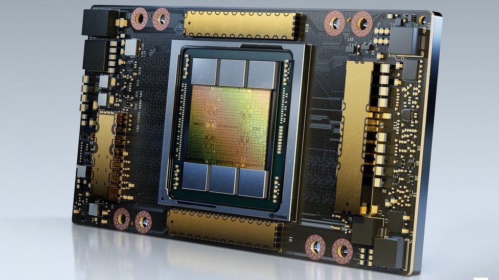
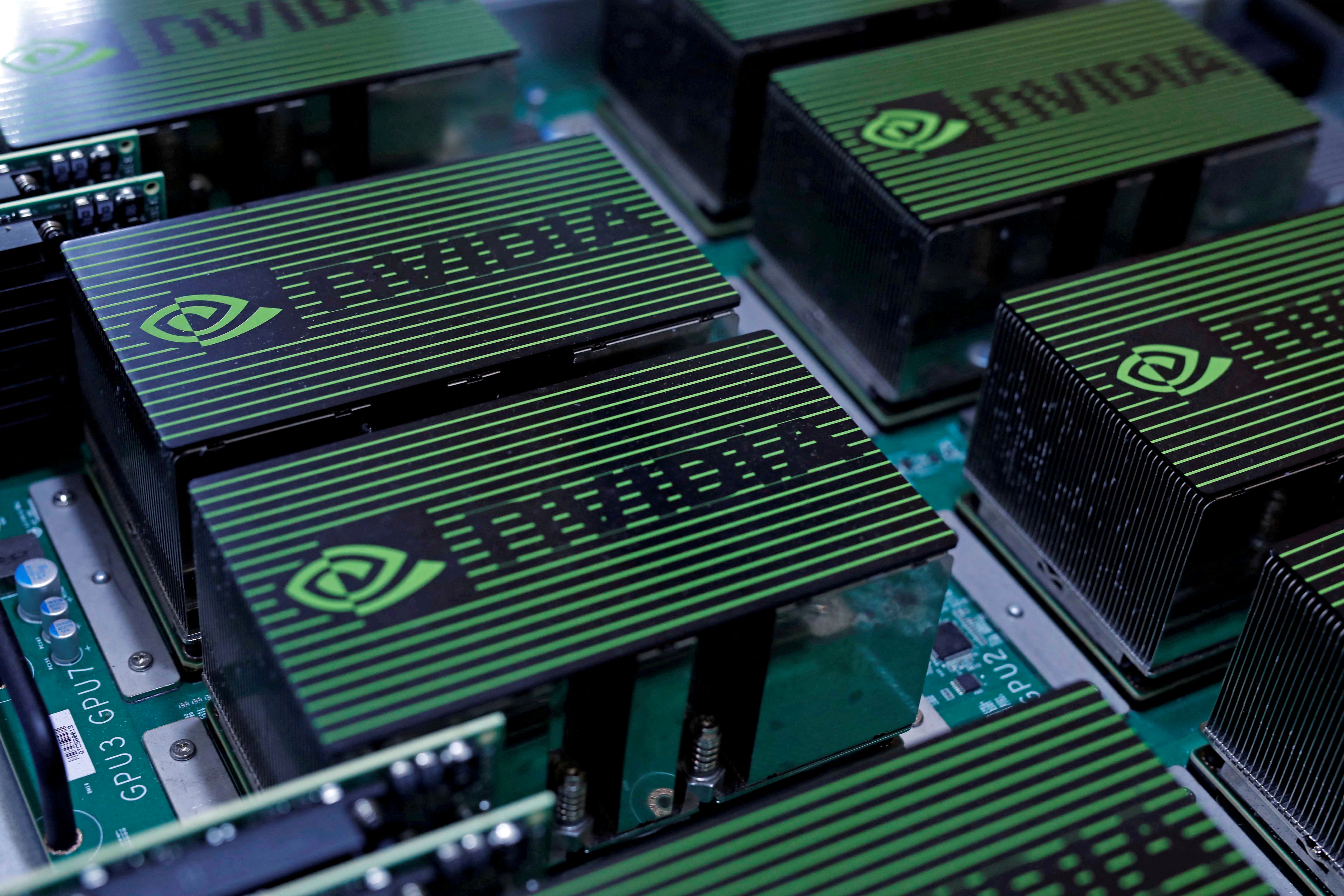
Their designs, ranging from consumer-grade GeForce and professional Quadro/RTX graphics cards to data center-focused Tesla and A100/H100 Tensor Core GPUs, represent the pinnacle of silicon engineering. Each generation introduces advancements in core count, memory bandwidth, specialized AI acceleration units (Tensor Cores), and interconnect technologies (NVLink). This relentless pursuit of performance and efficiency through design is what sets NVIDIA apart, making their intellectual property highly valuable and sought after by their manufacturing partners.
The Titans of Semiconductor Manufacturing: TSMC and Samsung
When it comes to fabricating NVIDIA’s cutting-edge designs, two names consistently emerge as the primary partners: Taiwan Semiconductor Manufacturing Company (TSMC) and Samsung Foundry. These two giants represent the pinnacle of semiconductor manufacturing capability, possessing the highly specialized equipment, expertise, and multi-billion-dollar fabs required to produce advanced chips at scale.
Taiwan Semiconductor Manufacturing Company (TSMC): The Industry Behemoth
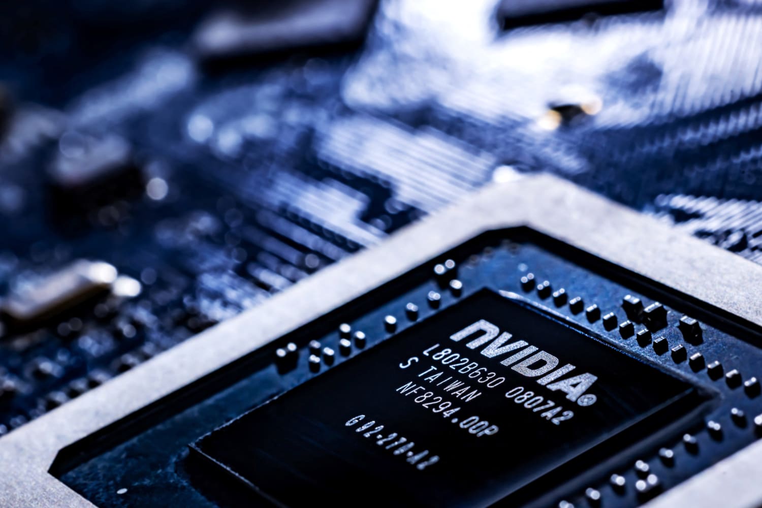
TSMC is, without a doubt, the world’s largest dedicated independent semiconductor foundry. Headquartered in Hsinchu, Taiwan, TSMC pioneered the pure-play foundry model and has maintained its leadership through continuous innovation and massive capital expenditure. Many of the world’s leading fabless companies, including Apple, Qualcomm, AMD, and NVIDIA, rely heavily on TSMC’s advanced process technologies.
NVIDIA has historically been a major customer of TSMC. For many generations of their GPUs, TSMC’s fabs in Taiwan have been responsible for translating NVIDIA’s intricate designs into physical silicon. This relationship is critical, as TSMC offers the most advanced process nodes (e.g., 5nm, 4nm, 3nm, and upcoming 2nm), which are essential for NVIDIA to achieve the performance, power efficiency, and transistor density required for their high-end GPUs and AI accelerators. The precision and consistency of TSMC’s manufacturing processes are legendary, enabling the complex multi-billion transistor designs that define modern high-performance computing.
The scale of TSMC’s operations is staggering, involving extreme ultraviolet (EUV) lithography machines, an army of highly skilled engineers, and a meticulously controlled manufacturing environment to produce defect-free chips. Their continuous investment in R&D ensures they remain at the forefront of process technology, a critical factor for NVIDIA to maintain its competitive edge.
Samsung Foundry: A Formidable Competitor and Integrated Giant
While TSMC often takes the lion’s share of NVIDIA’s most advanced orders, Samsung Foundry is another critical player in the manufacturing landscape. Part of the larger Samsung Electronics conglomerate, Samsung Foundry operates as an independent business unit offering foundry services to external customers, much like TSMC. However, unlike TSMC, Samsung Electronics also designs and manufactures its own chips (e.g., Exynos processors for smartphones, memory chips), making it an “integrated device manufacturer” (IDM) that also provides foundry services.
NVIDIA has utilized Samsung Foundry for certain product lines and generations. For instance, some reports indicate that NVIDIA utilized Samsung’s 8nm process for parts of its GeForce RTX 30 series (Ampere architecture). This strategic diversification can offer several benefits:
- Supply Chain Resilience: Relying on a single foundry carries inherent risks. Partnering with multiple foundries helps mitigate potential disruptions caused by geopolitical events, natural disasters, or manufacturing issues at a single plant.
- Negotiating Power: Having alternative manufacturing partners can provide NVIDIA with greater leverage during contract negotiations, potentially leading to better pricing or more favorable terms.
- Access to Different Technologies: While TSMC and Samsung compete fiercely on process nodes, each may offer unique optimizations or capabilities that align better with specific chip designs or market segments.
Samsung Foundry is also aggressively investing in advanced process technologies, including EUV lithography, and aims to compete head-to-head with TSMC in the most cutting-edge nodes. Their robust position in memory and packaging technologies further enhances their value proposition as a potential partner.
The Role of Advanced Process Nodes
The concept of “process nodes” (e.g., 7nm, 5nm, 3nm) refers to the generation of semiconductor manufacturing technology, often historically linked to the minimum feature size on a chip. While the naming convention is less directly related to physical dimensions today, these nodes represent critical advancements in transistor density, power efficiency, and performance. Each reduction in node size allows chip designers like NVIDIA to pack more transistors into the same area, or to create smaller, more power-efficient chips, leading to significant generational improvements in GPU performance and capability. The ability of TSMC and Samsung to deliver these increasingly smaller and more complex nodes is fundamental to NVIDIA’s ability to innovate.
The Complexities of the Semiconductor Supply Chain
While NVIDIA designs and foundries fabricate, the journey from raw silicon to a finished chip ready for integration into a graphics card or server involves a sprawling and intricate global supply chain far beyond just these two steps. This ecosystem encompasses specialized processes and numerous critical players.
Beyond Fabrication: Packaging, Assembly, and Testing (OSAT)
Once silicon wafers emerge from the foundry, covered with hundreds or thousands of individual chip “dies,” they are not yet ready for use. These wafers must undergo further processing, typically handled by Outsourced Semiconductor Assembly and Test (OSAT) companies.
- Wafer Dicing: The first step involves cutting the large silicon wafer into individual chip dies.
- Packaging: Each die is then encapsulated in a protective package, which provides electrical connections to the outside world (e.g., to a circuit board) and helps dissipate heat. This is a highly specialized field, with advanced packaging technologies like 2.5D (e.g., using interposers for HBM memory) and 3D stacking becoming increasingly crucial for high-performance chips. OSAT leaders include companies like ASE Technology Holding, Amkor Technology, and JCET.
- Assembly: This involves attaching the packaged chip onto a substrate, connecting it to other components like memory modules (e.g., High Bandwidth Memory – HBM) on a graphics card, and integrating it into the final product.
- Testing: Throughout the process, and especially at the end, rigorous testing is performed to ensure each chip functions correctly, meets performance specifications, and is free of defects. This can involve wafer-level testing, package-level testing, and final system-level validation. Any chip that fails these tests is discarded.
These OSAT processes are critical for the reliability, performance, and manufacturability of NVIDIA’s products, transforming raw silicon into a robust, functional component.
The Ecosystem of Equipment and Materials Suppliers
The entire semiconductor industry is underpinned by an even deeper layer of specialized suppliers. Without these companies, neither foundries nor OSAT providers could operate:
- Equipment Manufacturers: Companies like ASML (EUV lithography), Applied Materials, Lam Research, and Tokyo Electron provide the highly sophisticated and astronomically expensive machinery used in fabs for etching, deposition, lithography, and other processes. These machines are often unique and represent decades of R&D.
- Materials Suppliers: A vast array of companies supplies the ultra-pure silicon wafers, specialty gases, photoresists, chemicals, and other raw materials essential for chip fabrication. The purity and consistency of these materials are paramount to achieving high yields and reliable chip performance.
- EDA (Electronic Design Automation) Tools: Software companies like Synopsys and Cadence provide the sophisticated design tools and intellectual property (IP) blocks that NVIDIA engineers use to design their complex chips. These tools are indispensable for creating multi-billion transistor layouts.
Global Interdependencies and Geopolitical Implications
The semiconductor supply chain is profoundly globalized and highly interdependent. A single advanced chip can pass through multiple countries for different stages of its manufacturing journey: design in the US, fabrication in Taiwan or South Korea, packaging in Malaysia, and final assembly in China. This global distribution, while efficient, also creates vulnerabilities. Geopolitical tensions, trade disputes, and regional disruptions can have far-reaching impacts on the entire technology sector, as evidenced by recent chip shortages. The reliance on a few key players (like TSMC for advanced nodes) highlights the strategic importance of this industry and is driving discussions around supply chain diversification and domestic manufacturing initiatives.
Why Manufacturing Expertise Matters: Performance, Efficiency, and Innovation
The close collaboration between a fabless designer like NVIDIA and its foundry partners is a symbiotic relationship where the quality of manufacturing directly impacts the success of the chip design. The foundry’s expertise in process technology is not merely about producing chips, but about enabling NVIDIA’s ambitious performance and efficiency targets.
Driving Performance Through Process Technology
The performance of an NVIDIA GPU is not solely a function of its architectural design but also heavily dependent on the manufacturing process node used. Smaller nodes allow for:
- Higher Transistor Density: More transistors can be packed into a given die area, enabling more processing cores, more cache, and more complex functional units within the GPU. This directly translates to increased computational power.
- Faster Switching Speeds: Smaller transistors can switch on and off more quickly, leading to higher clock frequencies and improved overall chip speed.
- Reduced Parasitic Capacitance: Less resistance and capacitance between transistors means signals travel faster and consume less power.
Without access to cutting-edge process technology from its foundry partners, NVIDIA would struggle to deliver the generational performance improvements that its customers expect and that are necessary to maintain its leadership in graphics and AI.
Energy Efficiency and Die Size Optimization
Beyond raw performance, energy efficiency is a critical metric for modern chips, especially for data centers and mobile applications. Advanced process nodes enable:
- Lower Power Consumption: Smaller transistors require less voltage to operate, significantly reducing power consumption. This is crucial for managing heat, extending battery life in mobile devices, and reducing operating costs in massive data centers.
- Smaller Die Sizes: More transistors in a smaller area mean a smaller die size. This has economic benefits, as more chips can be cut from a single silicon wafer, reducing the cost per chip. It also allows for more compact designs in final products.
NVIDIA’s ability to create powerful yet energy-efficient chips is a direct testament to the capabilities of its manufacturing partners.
The Race for Next-Generation Foundries
The competition among foundries to achieve the next major process node (e.g., from 3nm to 2nm) is relentless and requires colossal investments in R&D and equipment. NVIDIA, along with other leading chip designers, is often involved in early collaboration with foundries to optimize their designs for upcoming nodes. This co-optimization ensures that the chips leverage the full potential of the new manufacturing process, achieving optimal performance and yield. The “process roadmap” of TSMC and Samsung is a critical consideration for NVIDIA’s own product roadmap, as their future chip architectures are often designed with specific upcoming process nodes in mind.
Future Outlook: Diversification, Resilience, and Onshoring Efforts
The lessons learned from recent global events, particularly the COVID-19 pandemic and geopolitical tensions, have highlighted the vulnerabilities of the highly concentrated semiconductor supply chain. This is prompting a shift towards greater diversification and resilience, with NVIDIA and its partners playing a key role.
Geographical Diversification Strategies
While Taiwan and South Korea remain global hubs for advanced chip manufacturing, there is increasing pressure and strategic impetus to diversify manufacturing geographically. Both TSMC and Samsung are responding to this by establishing new fabs in other regions:
- TSMC in the US and Japan: TSMC is building new advanced fabs in Arizona, USA, and expanding its presence in Japan. These moves are partly driven by government incentives and customer demand for localized production.
- Samsung in the US: Samsung Foundry is also investing heavily in expanding its US manufacturing footprint, with significant plans for new fabs in Texas.
For NVIDIA, these initiatives could eventually lead to more geographically diverse sourcing options for their future chips, potentially reducing lead times and strengthening supply chain security.
The Quest for Supply Chain Resilience
Beyond geographical spread, true supply chain resilience involves multiple layers:
- Dual Sourcing: Partnering with multiple foundries (like TSMC and Samsung) for different products or even different process nodes of the same product.
- Inventory Management: Maintaining strategic inventories of critical components.
- Advanced Analytics: Using data to predict and mitigate potential disruptions.
NVIDIA actively works with its suppliers to optimize its supply chain for both efficiency and robustness, ensuring it can continue to deliver its high-demand products even amidst global challenges.
The Role of Government Subsidies and National Security
Governments worldwide, recognizing the strategic importance of semiconductors, are implementing policies and providing massive subsidies to encourage domestic chip manufacturing. Initiatives like the CHIPS Act in the United States and similar programs in Europe and Japan aim to:
- Reduce Reliance on Overseas Fabs: Particularly for critical infrastructure and defense applications.
- Create Jobs and Foster Innovation: Boosting domestic high-tech industries.
- Enhance Economic Security: Ensuring a reliable supply of chips for a wide range of industries.
While these efforts will take years, even decades, to significantly alter the global landscape, they represent a fundamental shift towards a more distributed and potentially resilient semiconductor ecosystem. NVIDIA, as a leading designer, will undoubtedly benefit from a stronger, more diversified manufacturing base as these investments mature, ensuring the continued availability of the high-performance chips that drive the technological future.
aViewFromTheCave is a participant in the Amazon Services LLC Associates Program, an affiliate advertising program designed to provide a means for sites to earn advertising fees by advertising and linking to Amazon.com. Amazon, the Amazon logo, AmazonSupply, and the AmazonSupply logo are trademarks of Amazon.com, Inc. or its affiliates. As an Amazon Associate we earn affiliate commissions from qualifying purchases.