
For anyone tracking the trajectory of modern computing, the question of where NVIDIA is headquartered leads directly to the epicenter of the global semiconductor and artificial intelligence industry. NVIDIA is headquartered at 2788 San Tomas Expressway in Santa Clara, California. While the address is a specific point on a map, the physical campus represents far more than just a corporate office; it is a meticulously engineered environment designed to foster the next generation of accelerated computing and generative AI.
Situated in the heart of Silicon Valley, the NVIDIA headquarters serves as a physical manifestation of the company’s transition from a niche graphics card manufacturer to the most influential player in the global technology ecosystem. As we explore the technical and strategic significance of this location, we find a campus that is built with the same “first principles” approach that NVIDIA applies to its GPU architectures.
The Silicon Valley Epicenter: Why Santa Clara Matters for Tech Innovation
The choice of Santa Clara as NVIDIA’s home base is no historical accident. As part of the Santa Clara Valley, this region has been the bedrock of semiconductor development since the 1960s. By positioning itself here, NVIDIA sits within a dense web of technological interdependency that includes hardware manufacturers, software giants, and elite research institutions.
The Proximity to the Semiconductor Legacy
Santa Clara is the home of the “Silicon” in Silicon Valley. NVIDIA’s headquarters is located just miles away from other industry titans such as Intel and AMD. This proximity creates a unique tech corridor where the exchange of ideas, talent, and specialized labor occurs at a velocity found nowhere else on earth. For NVIDIA, being in Santa Clara means being at the center of the supply chain conversations and engineering standards that dictate how modern servers and data centers are built.
A Hub for Global Tech Talent
One of the primary technical advantages of NVIDIA’s headquarters location is its proximity to Stanford University and the University of California, Berkeley. These institutions are the primary feeders for the deep learning and computer science talent that NVIDIA requires to develop its CUDA platform and Blackwell architectures. The Santa Clara headquarters acts as a magnet, drawing in the world’s leading experts in parallel processing, ray tracing, and neural networks, all of whom reside within the surrounding Bay Area ecosystem.
Architectural Engineering: The “Endeavor” and “Voyager” Campuses
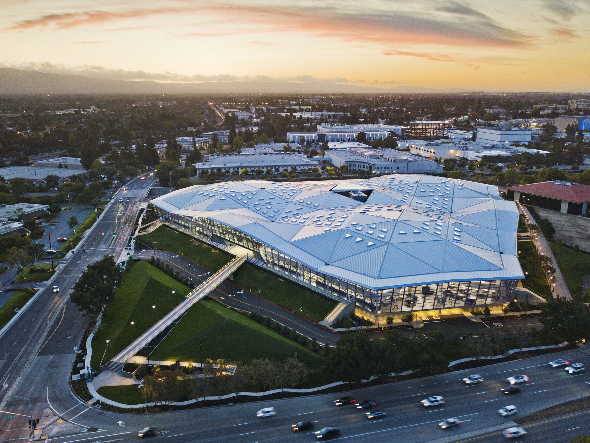
NVIDIA’s headquarters is comprised of two primary landmark buildings: Endeavor and Voyager. These structures are not merely office spaces; they are highly specialized environments designed to optimize human interaction and engineering workflows. Jensen Huang, NVIDIA’s CEO, envisioned a workspace that mirrored the complexity and efficiency of a high-performance chip.
Designing for “Collisions” and Collaboration
The “Endeavor” building, a 500,000-square-foot structure completed in 2017, and its successor, “Voyager,” were designed by the architectural firm Gensler with a specific tech-centric philosophy. The interior layout avoids traditional silos and cubicles. Instead, it utilizes a “non-hierarchical” design that encourages “accidental collisions.” In the world of complex software engineering and hardware design, these spontaneous interactions between different teams—such as the networking experts and the GPU architects—are where breakthroughs in system-on-chip (SoC) integration often occur.
The Triangle: The Fundamental Building Block
A fascinating technical detail of the NVIDIA headquarters is the recurring use of the triangle in its architectural design. In computer graphics, the triangle is the fundamental primitive used to render complex 3D shapes. The roofline of the Endeavor building is composed of a series of interlocking triangles, a nod to NVIDIA’s roots in geometry processing. This design isn’t just aesthetic; the geometric skylights are engineered to flood the interior with natural light while minimizing heat gain, reflecting the company’s focus on power efficiency—a critical metric in both architectural design and GPU TDP (Thermal Design Power) management.

Technical Infrastructure and the AI Labs
Beyond the glass and steel of the exterior, the NVIDIA headquarters houses some of the most advanced private research laboratories in the world. As the company has shifted its focus toward data-center-scale computing, the infrastructure at 2788 San Tomas Expressway has evolved to support massive internal compute clusters.
On-Site Data Centers and Prototyping
NVIDIA’s Santa Clara campus serves as a primary site for the early-stage testing of their DGX systems. Before a new H100 or B200 cluster is deployed to global cloud providers like AWS or Azure, the hardware and software integration is often perfected within the labs at the headquarters. The facility is equipped with specialized power and cooling infrastructure to handle the immense thermal output of modern AI supercomputers, allowing engineers to run “real-world” stress tests on upcoming silicon.
The Robotics and Simulation Labs
A significant portion of the headquarters is dedicated to the development of NVIDIA Isaac and the Omniverse platform. These labs are equipped with high-fidelity sensors and robotic arms where engineers work on bridging the gap between “Silicon and Carbon.” Here, the digital twin technology is perfected, allowing researchers to simulate complex physics environments in a virtual space before deploying the code to physical machines. The headquarters acts as the central node for this “Sim-to-Real” pipeline, which is essential for the future of autonomous vehicles and industrial automation.
The Strategic Importance of the San Tomas Corridor
The location of NVIDIA’s headquarters along the San Tomas Expressway provides more than just easy highway access; it places the company at the heart of the “AI infrastructure” map.
Integration with the Software Ecosystem
While NVIDIA is a hardware company at its core, its dominance is maintained through its software stack, particularly CUDA. The headquarters is the nerve center for thousands of software engineers who write the libraries that power modern AI. Being located in Santa Clara allows for seamless integration with the software ecosystems of nearby companies like Google (Mountain View) and Meta (Menlo Park). The low-latency collaboration between NVIDIA’s driver teams and the world’s leading AI model developers is a key reason why the “NVIDIA standard” remains the industry benchmark.
Sustainable Tech Operations
In line with modern tech standards, the Voyager building is a model of sustainable engineering. It features a massive solar trellis and a reclaimed water system. For a company that is often criticized for the power consumption of AI, the headquarters serves as a showcase for how large-scale tech operations can move toward carbon neutrality. The building’s smart systems use AI-driven climate control, showcasing NVIDIA’s own technology being used to optimize the energy efficiency of the very space where that technology is invented.

Conclusion: A Physical Landmark for a Digital Future
To understand “where” NVIDIA is headquartered is to understand the geography of the future. While the company has offices in over 50 locations worldwide—from research centers in Israel to engineering hubs in Taiwan—the Santa Clara campus remains the undisputed “brain” of the operation.
The 2788 San Tomas Expressway address is more than just a corporate headquarters; it is a high-tech foundry of ideas. From the triangle-patterned roofs that echo the origins of 3D rendering to the advanced labs where the next generation of Blackwell chips are tested, every square inch of the campus is designed to accelerate the evolution of technology. In the fast-moving world of AI, where a single year can see a decade’s worth of progress, NVIDIA’s headquarters provides the stable, specialized environment necessary to sustain the most ambitious engineering projects of the 21st century.
Whether you view it as a landmark of Silicon Valley history or the cockpit of the AI revolution, NVIDIA’s Santa Clara home is where the digital world’s most complex problems are being solved, one GPU at a time.
aViewFromTheCave is a participant in the Amazon Services LLC Associates Program, an affiliate advertising program designed to provide a means for sites to earn advertising fees by advertising and linking to Amazon.com. Amazon, the Amazon logo, AmazonSupply, and the AmazonSupply logo are trademarks of Amazon.com, Inc. or its affiliates. As an Amazon Associate we earn affiliate commissions from qualifying purchases.