
The question “where are Intel chips manufactured” might seem straightforward, but its answer reveals a complex, globally interconnected web of advanced technology, geopolitical strategy, and intricate supply chains. Far from being confined to a single location, the journey of an Intel chip from raw silicon to a functional component powering our devices spans continents, involving highly specialized facilities and a collaborative network of partners. Understanding this landscape is crucial for appreciating the technological prowess required to produce the semiconductors that underpin the modern digital world.
Intel, for decades, operated predominantly as an Integrated Device Manufacturer (IDM), meaning it designed, manufactured, and packaged its own chips. This vertical integration was a hallmark of its strategy and a source of immense competitive advantage. However, in response to evolving market dynamics, escalating manufacturing costs, and the rise of advanced foundry services like TSMC and Samsung, Intel has embarked on a transformative journey, aptly named IDM 2.0. This new strategy involves a hybrid approach, leveraging both its robust internal manufacturing capabilities and increasingly, external foundries, while also establishing its own foundry services for other companies. This shift not only diversifies where Intel chips are made but also fundamentally alters Intel’s role in the broader semiconductor ecosystem.

Intel’s Evolving Manufacturing Strategy: From IDM to IDM 2.0
For much of its history, Intel embodied the Integrated Device Manufacturer (IDM) model, a vertically integrated structure where the company controlled every stage of chip production—from design and research to fabrication, assembly, test, and packaging. This comprehensive control was a cornerstone of Intel’s innovation and quality assurance, allowing for tight integration between design and process technology. The IDM model, while offering significant advantages in performance optimization and intellectual property protection, also presented challenges in terms of capital expenditure and the sheer complexity of maintaining state-of-the-art manufacturing facilities across multiple generations of technology.
The Traditional IDM Model: A Legacy of Vertical Integration
Historically, Intel’s operational philosophy dictated that it would design, develop, and manufacture its processors entirely within its own ecosystem. This meant massive investments in research and development for process technology, building and equipping cutting-edge fabrication plants (fabs), and establishing extensive assembly and test operations. This approach allowed Intel to optimize its chip designs directly for its proprietary manufacturing processes, often leading to performance advantages and a tighter feedback loop between design and manufacturing teams. Major production facilities were primarily located in strategic regions known for technological infrastructure and skilled labor, particularly the United States and Ireland. This model fostered a deep institutional knowledge in semiconductor manufacturing that few companies could rival.
The Shift to IDM 2.0: A Hybrid Approach for the Future
Facing intensifying competition, the soaring costs of developing leading-edge process technologies, and the need for greater flexibility, Intel announced its IDM 2.0 strategy in 2021. This strategic pivot marks a significant departure from its pure IDM roots, embracing a more hybrid model. IDM 2.0 has three core components:
- Internal Manufacturing: Intel continues to operate and expand its world-class internal factory network for the bulk of its product volume. This remains the backbone of its manufacturing capability.
- External Foundry Use: For certain products and specific technology nodes, Intel is increasingly leveraging external foundries (like TSMC) to manufacture a portion of its chips. This provides access to advanced process technologies without the immediate capital outlay and reduces the pressure on internal fabs.
- Intel Foundry Services (IFS): Perhaps the most significant change, Intel is opening its own fabs to produce chips for other companies, essentially becoming a foundry competitor. This strategic move aims to leverage Intel’s manufacturing scale and process expertise, turning a cost center into a potential revenue stream and positioning Intel as a key player in the global foundry market.
This shift signifies a recognition that a flexible, multi-faceted manufacturing strategy is essential for navigating the complexities of the modern semiconductor industry. It means that while many Intel chips are still “Made by Intel,” an increasing number might be “Designed by Intel, Manufactured by TSMC,” or even “Designed by Company X, Manufactured by Intel.”
Key Manufacturing Hubs and Global Presence
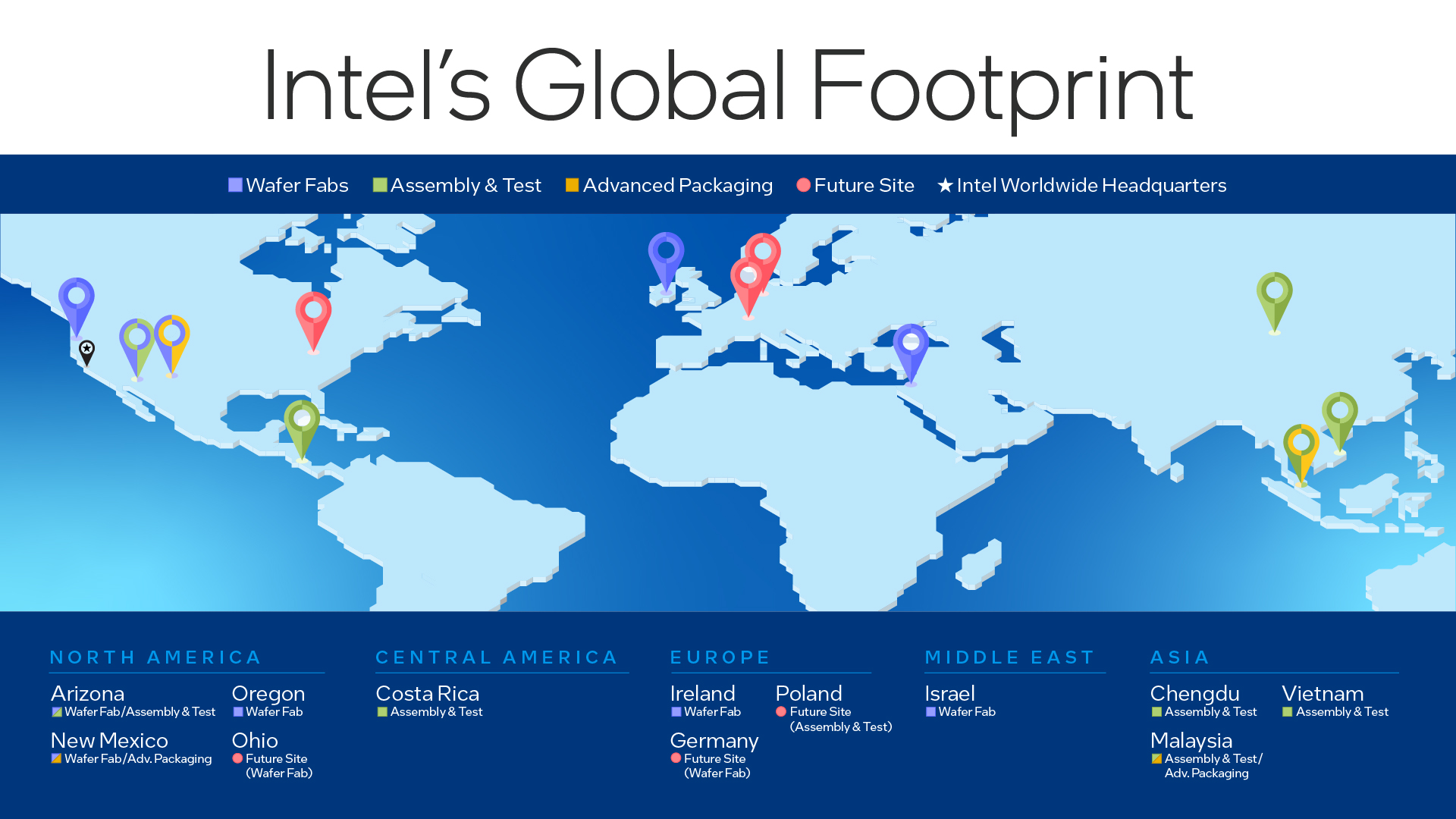
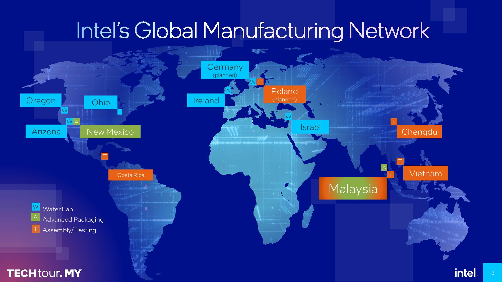
Intel’s manufacturing footprint is vast, reflecting the enormous investment and specialized infrastructure required for semiconductor fabrication. These facilities, known as “fabs,” are among the most advanced and expensive industrial sites on the planet, often costing tens of billions of dollars to build and equip. They operate 24/7 in ultra-clean environments, utilizing sophisticated machinery and highly skilled personnel to transform raw silicon wafers into intricate microprocessors.
Manufacturing in the United States: Core of Intel’s Fabrication
The United States has historically been and remains a critical cornerstone of Intel’s manufacturing operations. Intel operates several advanced fabrication plants across various states, representing a significant portion of its global output and R&D efforts.
- Oregon (Ronler Acres Campus): This campus near Portland is Intel’s primary R&D site for process technology development. It often hosts the first fabs to implement a new generation of manufacturing processes, proving out the technology before it’s deployed globally. It’s a critical hub for innovation.
- Arizona (Ocotillo Campus): Located in Chandler, Arizona, this facility is one of Intel’s largest manufacturing sites, featuring multiple fabs producing a wide range of processors. Arizona has seen significant expansion efforts, including new investments announced as part of the IDM 2.0 strategy to boost domestic manufacturing capacity.
- New Mexico (Rio Rancho Campus): This site traditionally focused on packaging and assembly, but has also performed some fabrication. It remains a key facility for advanced packaging technologies, which are becoming increasingly critical for chip performance.
These U.S. facilities are not just production sites; they are strategic assets vital for national security and technological leadership, often receiving significant government incentives.
European Operations: Expanding Capacity and Strategic Investment
Europe plays an increasingly important role in Intel’s manufacturing landscape, particularly in recent years as part of a broader strategy to diversify supply chains and strengthen regional capabilities.
- Ireland (Leixlip Campus): Intel’s European base in Leixlip, County Kildare, has been a significant manufacturing hub for decades, producing chips for various markets. It has seen substantial investment and upgrades, becoming a critical part of Intel’s global network, especially for advanced process nodes.
- Germany (Magdeburg Project): In a landmark decision, Intel announced plans to build a “mega-fab” complex in Magdeburg, Germany. This multi-billion-euro investment is set to become one of Europe’s largest semiconductor manufacturing sites, crucial for bolstering European chip production and reducing reliance on Asian supply chains. This project is a cornerstone of Intel’s commitment to IDM 2.0 and regionalization.
Israeli Innovation Hubs and Southeast Asian Assembly
Beyond the primary fabrication sites, Intel’s global presence extends to other critical regions for different stages of the chip lifecycle.
- Israel (Kiryat Gat): While known more for its design and R&D centers, Intel also operates a fabrication facility in Kiryat Gat, Israel. This site has been instrumental in producing advanced chips and often contributes to the development and refinement of new process technologies, making it a key part of Intel’s global manufacturing footprint.
- Southeast Asia (Malaysia, Vietnam): Once chips are fabricated, they need to be assembled, tested, and packaged. Intel has extensive operations for these crucial final stages in Southeast Asian countries like Malaysia and Vietnam. These facilities are responsible for transforming silicon wafers into finished, ready-to-use microprocessors, ensuring their quality and reliability before they reach consumers and enterprises. The cost-efficiency and established infrastructure in these regions make them ideal for these high-volume, labor-intensive processes.
The Global Semiconductor Supply Chain and Geopolitical Implications
The journey of an Intel chip, from raw material to a finished product, is a testament to the immense complexity and globalized nature of the semiconductor supply chain. This chain involves hundreds of companies across dozens of countries, each specializing in a particular stage or component. This intricate web is increasingly subject to geopolitical forces, as nations recognize the strategic importance of semiconductor independence.
From Sand to Silicon: The Raw Materials and Wafer Production
The starting point for any silicon chip is incredibly pure silicon, typically extracted from quartz sand. This raw material undergoes extensive purification to create electronic-grade silicon, which is then grown into large, single-crystal ingots. These ingots are sliced into thin, perfectly smooth silicon wafers, which serve as the substrate upon which integrated circuits are built. Companies specializing in these initial stages, such as Shin-Etsu Chemical and SUMCO, are often based in Japan and other Asian countries, forming a foundational layer of the supply chain. Any disruption at this nascent stage can have ripple effects across the entire industry.
The Lithography Challenge: Precision at the Atomic Scale
The heart of chip manufacturing lies in photolithography, a process where intricate circuit patterns are etched onto the silicon wafer using light. This requires extremely advanced equipment, most notably the steppers and scanners produced by companies like ASML from the Netherlands. ASML holds a near-monopoly on Extreme Ultraviolet (EUV) lithography machines, which are essential for manufacturing the most advanced chips with nanometer-scale features. Without access to these machines, producing leading-edge processors like those from Intel would be impossible. This concentration of critical technology in a single company highlights a significant choke point in the global supply chain, making it a subject of international policy and trade discussions.
Assembly, Test, and Packaging (ATP): The Final Frontier
Once the complex circuits are fabricated onto the silicon wafers, the wafers are sent to Assembly, Test, and Packaging (ATP) facilities. Here, the wafers are cut into individual dies (the actual chips), which are then meticulously assembled into packages that protect them, provide electrical connections, and allow them to be mounted onto circuit boards. Each chip undergoes rigorous testing to ensure it meets performance and reliability specifications. Major players in this segment include ASE Group and Amkor Technology, with significant operations in Taiwan, China, Malaysia, and other Southeast Asian nations. These final stages are labor-intensive and require precision engineering, making regional specialization economically viable.
The Importance of Redundancy and Reshoring Initiatives
The COVID-19 pandemic and subsequent supply chain disruptions exposed the fragility of a highly optimized, just-in-time global semiconductor ecosystem. This vulnerability, coupled with escalating geopolitical tensions (particularly between the U.S. and China), has spurred governments worldwide to pursue “reshoring” or “friend-shoring” initiatives. Countries like the United States (with the CHIPS Act) and the European Union (with the European Chips Act) are investing billions of dollars in subsidies and incentives to bring semiconductor manufacturing, including Intel’s new fabs, back to their shores. The goal is to build redundancy, enhance national security, and reduce reliance on single points of failure, thereby creating a more resilient and geographically diversified supply chain for vital technologies.
Challenges and The Future of Chip Manufacturing
The semiconductor industry stands at a critical juncture, facing unprecedented technological, economic, and geopolitical challenges. The future of where and how Intel chips are manufactured will be shaped by these evolving dynamics, demanding continuous innovation and strategic adaptation.
The Race for Advanced Nodes: Pushing the Limits of Physics
The relentless pursuit of smaller, faster, and more power-efficient chips drives the industry towards ever more advanced manufacturing nodes (e.g., 5nm, 3nm, 2nm). Each new node requires colossal R&D investment, new materials, and highly sophisticated manufacturing techniques, pushing the very limits of physics and engineering. Intel, with its “five nodes in four years” strategy (Intel 7, Intel 4, Intel 3, Intel 20A, Intel 18A), is aggressively striving to regain its process technology leadership. This race is not just about performance; it’s about economic competitiveness and geopolitical influence, as control over leading-edge fabrication is a powerful strategic asset. The cost of developing these nodes means fewer companies can afford to compete, further concentrating manufacturing capability.
Geopolitical Tensions and the Push for Regionalization
Geopolitical tensions, particularly between major global powers, are profoundly impacting semiconductor manufacturing. The strategic importance of chips, often dubbed “the new oil,” has led to export controls, trade restrictions, and an accelerated drive for regional self-sufficiency. Nations are keen to reduce their dependence on offshore manufacturing, especially for critical infrastructure and defense applications. This push for regionalization, while enhancing supply chain resilience, also increases manufacturing costs and potentially fragments the global technology landscape. Intel’s investments in the U.S. and Germany are direct responses to these geopolitical imperatives, aligning with government initiatives to localize advanced manufacturing.
Environmental Sustainability in Chip Production
Semiconductor manufacturing is an incredibly resource-intensive process, consuming vast amounts of energy and water, and generating significant waste. As environmental concerns escalate, the industry faces increasing pressure to adopt more sustainable practices. This includes reducing carbon emissions, optimizing water usage, minimizing hazardous waste, and sourcing renewable energy. Intel has set ambitious goals for environmental sustainability, investing in green technologies and processes across its fabs. Future manufacturing sites will likely incorporate advanced environmental controls and sustainable design principles, balancing technological progress with ecological responsibility.
Talent Development and Investment in the Future Workforce
The highly specialized nature of semiconductor manufacturing requires a continuous supply of skilled engineers, scientists, and technicians. The global shortage of such talent poses a significant challenge, particularly as new fabs are built and older ones are upgraded. Investing in education, workforce development programs, and STEM initiatives is crucial to ensure a pipeline of qualified personnel. Governments and companies, including Intel, are collaborating to bridge this skills gap, recognizing that human capital is as vital as technological capital in maintaining manufacturing leadership.
In conclusion, the question of where Intel chips are manufactured unveils a dynamic and evolving global ecosystem. From its traditional IDM roots primarily centered in the U.S. and Ireland, Intel is rapidly transforming into an IDM 2.0 powerhouse, leveraging a diversified manufacturing footprint that includes expanding domestic fabs, strategic international sites like Germany and Israel, and the innovative Intel Foundry Services. This complex web reflects not just technological advancements but also profound geopolitical shifts, economic imperatives, and a collective drive towards a more resilient and regionally balanced semiconductor supply chain. The future of Intel’s manufacturing will continue to be a fascinating interplay of cutting-edge technology, global strategy, and an unwavering commitment to innovation.
aViewFromTheCave is a participant in the Amazon Services LLC Associates Program, an affiliate advertising program designed to provide a means for sites to earn advertising fees by advertising and linking to Amazon.com. Amazon, the Amazon logo, AmazonSupply, and the AmazonSupply logo are trademarks of Amazon.com, Inc. or its affiliates. As an Amazon Associate we earn affiliate commissions from qualifying purchases.