
In the current landscape of global innovation, few companies hold as much influence over our daily lives as the Taiwan Semiconductor Manufacturing Company, better known as TSMC. While brands like Apple, Nvidia, and Sony capture the public’s imagination with sleek gadgets and powerful graphics cards, it is TSMC that builds the “brains” inside these devices. As the world’s largest and most advanced dedicated semiconductor foundry, TSMC is the invisible backbone of the digital age.
To understand TSMC is to understand the history and future of computing itself. From the smartphone in your pocket to the massive data centers powering Artificial Intelligence (AI), TSMC’s mastery of silicon fabrication has made it an indispensable pillar of the global technology ecosystem.

The Foundation of Modern Computing: The Pure-Play Foundry Model
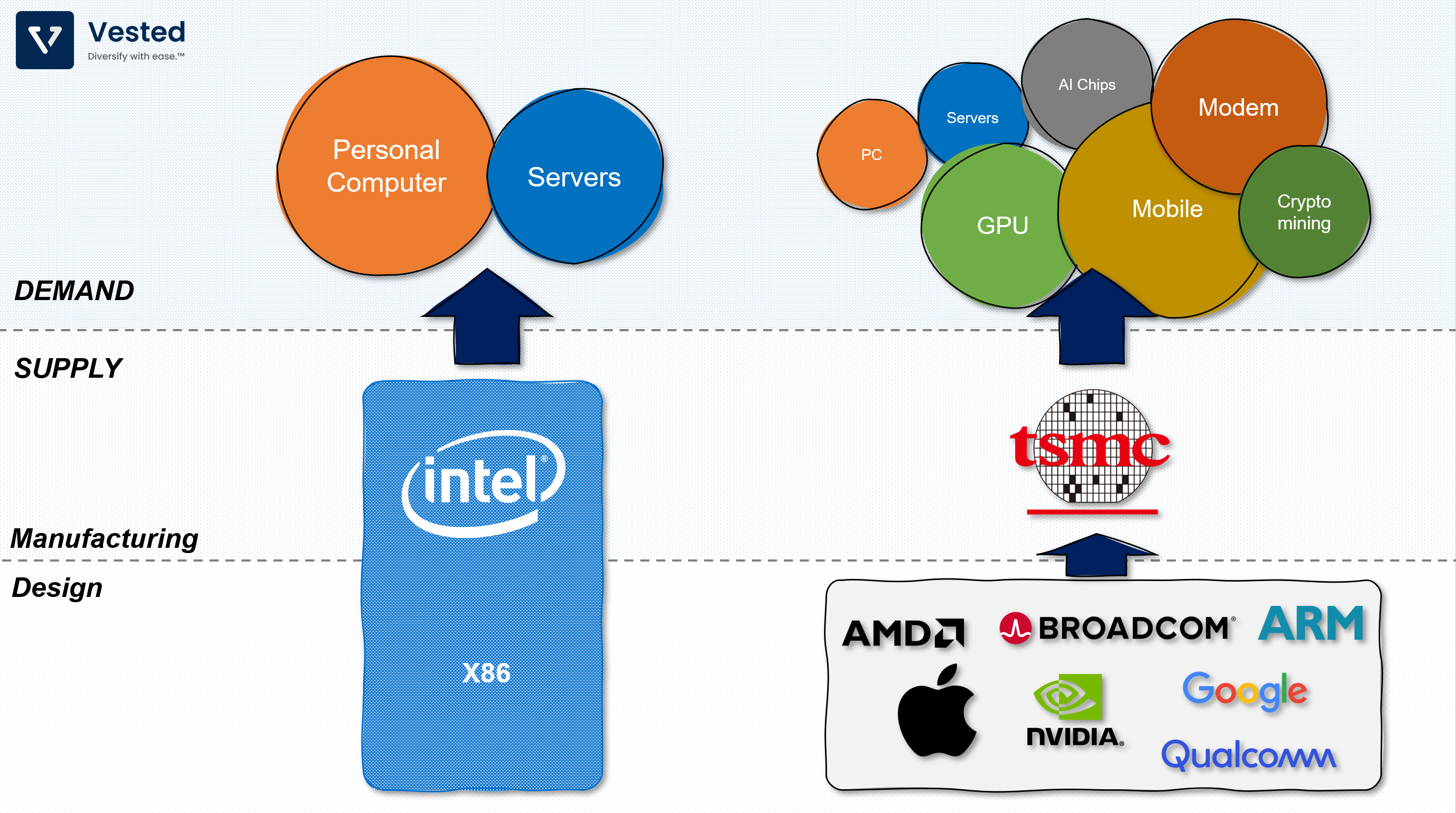
Before TSMC was founded in 1987 by Morris Chang, the semiconductor industry operated under a vastly different paradigm. Companies that designed chips—such as Intel or Motorola—also owned the factories (fabs) that manufactured them. This required immense capital investment, making it nearly impossible for small startups to innovate in the hardware space.
Redefining Chip Manufacturing
TSMC’s revolutionary contribution was the “pure-play foundry” model. Morris Chang realized that if a company focused solely on manufacturing chips for others, rather than designing its own products, it could achieve economies of scale and serve a diverse range of clients. TSMC does not sell its own brand of processors; instead, it provides the manufacturing expertise and infrastructure for the world’s leading technology designers.
By focusing exclusively on the manufacturing process, TSMC eliminated the “conflict of interest” inherent in the industry. Clients like Apple or AMD could hand over their secret blueprints to TSMC, knowing that the foundry wouldn’t use that intellectual property to compete with them in the consumer market. This trust built the foundation for a collaborative ecosystem that accelerated the pace of global innovation.
The Fabless Revolution
The rise of TSMC gave birth to the “fabless” semiconductor movement. Companies like Qualcomm, Nvidia, and MediaTek were able to flourish because they didn’t need to spend billions of dollars building their own factories. They could focus entirely on architectural design and software optimization, leaving the complex physics of silicon etching to TSMC. This specialization has led to the rapid advancement of mobile computing, high-performance gaming, and specialized AI hardware over the last three decades.
Leading the Global Race: Process Nodes and Miniaturization
In the world of technology, performance is often measured by how many transistors can be packed onto a tiny sliver of silicon. This is governed by “nodes,” which traditionally referred to the physical size of the components on a chip. Today, TSMC is the undisputed leader in this “nanometer race.”
The Mastery of Nanometer Technology
TSMC’s dominance is defined by its ability to mass-produce chips at the 5-nanometer (nm), 3nm, and soon, 2nm scales. To put this in perspective, a human hair is roughly 80,000 to 100,000 nanometers wide. At the 3nm level, TSMC is manipulating matter at a near-atomic scale.
Smaller nodes allow for more transistors on a single chip, which translates directly to two things: higher performance and better energy efficiency. This is why a modern smartphone has more computing power than the rooms full of computers used for the Apollo moon missions. TSMC’s ability to yield high-quality wafers at these microscopic scales is what allows tech giants to claim “30% faster speeds” or “all-day battery life” with every new product generation.
Extreme Ultraviolet (EUV) Lithography
The secret weapon in TSMC’s technical arsenal is its early and aggressive adoption of Extreme Ultraviolet (EUV) lithography. Manufacturing chips at the 7nm node and below requires light with an incredibly short wavelength to “print” circuit patterns onto silicon wafers.
EUV machines, manufactured primarily by the Dutch firm ASML, are some of the most complex pieces of equipment ever created by humanity. TSMC’s mastery over EUV technology has allowed it to pull ahead of competitors like Intel and Samsung. By perfecting the use of these machines, TSMC has maintained a “process lead,” ensuring that the most advanced chips in the world can only be made in their facilities.
Powering the AI and Smartphone Era
TSMC’s client list reads like a “Who’s Who” of the tech industry. Because the company sits at the top of the pyramid in terms of manufacturing capability, the biggest names in tech are in a constant queue to secure TSMC’s production capacity.
Apple, Nvidia, and the 3nm Frontier
Apple is perhaps TSMC’s most famous partner. The transition of the Mac lineup to “Apple Silicon” (the M-series chips) was only possible because of TSMC’s advanced nodes. By utilizing TSMC’s 5nm and 3nm processes, Apple was able to create laptops that offered industry-leading performance with significantly lower heat and power consumption than traditional x86 processors.
Similarly, the current boom in Generative AI would be impossible without TSMC. Nvidia’s H100 and B200 Blackwell chips—the engines behind platforms like ChatGPT—are manufactured by TSMC. These AI accelerators require massive amounts of transistors and specialized packaging technology (known as CoWoS) that TSMC has spent decades perfecting. Without TSMC’s ability to scale these complex designs, the AI revolution would effectively stall.
Specialized Solutions for Automotive and IoT
While the “leading edge” (3nm and 5nm) gets the headlines, TSMC also produces a vast array of “specialty” chips. These are used in the automotive industry for electric vehicle management and autonomous driving sensors, as well as in Internet of Things (IoT) devices. Modern cars are essentially “computers on wheels,” and TSMC’s specialized high-voltage and high-reliability processes ensure that these chips can survive the harsh environments of a vehicle’s engine bay for decades.
The Strategic Importance of the “Silicon Shield”
TSMC is not just a technology company; it is a geopolitical heavyweight. Based in Hsinchu, Taiwan, the company’s concentration of high-tech manufacturing has created what many call the “Silicon Shield.”
Geopolitical Significance and Supply Chain Resilience
Because the entire global economy—from fighter jets to washing machines—relies on chips produced by TSMC, the world has a vested interest in the stability and security of Taiwan. A disruption in TSMC’s production would likely result in a global economic depression, as there is currently no other company capable of absorbing their production volume or matching their technical sophistication.
This “single point of failure” in the global supply chain has led to a renewed focus on semiconductor sovereignty. Governments in the United States, Europe, and Japan are now offering billions of dollars in subsidies to encourage TSMC to diversify its manufacturing footprint.
Global Expansion: Fab 21 and Beyond
In response to these global pressures, TSMC has begun an ambitious international expansion. This includes the construction of “Fab 21” in Arizona, USA, and new facilities in Kumamoto, Japan, and Dresden, Germany. These projects represent some of the largest foreign direct investments in history.
However, TSMC’s core research and development and its most advanced “pioneer” nodes remain in Taiwan. The logistical challenge of replicating the “Hsinchu ecosystem”—where suppliers, engineers, and testing facilities are all within a few miles of each other—is one of the greatest technical hurdles the company faces as it goes global.
The Future of Semiconductors: Beyond Moore’s Law
As we approach the physical limits of silicon, TSMC is looking toward the next frontier of materials science and chip architecture. The industry is currently grappling with the slowing of Moore’s Law—the observation that the number of transistors on a chip doubles roughly every two years.
2nm, 1.4nm, and Gate-All-Around (GAA)
TSMC’s roadmap includes the move to “2nm” production by 2025. This transition will involve a shift from the traditional “FinFET” transistor architecture to a new design called “Gate-All-Around” (GAA) or nanosheet transistors. This new architecture allows for even finer control over electrical current, reducing leakage and enabling further performance gains. Beyond 2nm, TSMC is already researching the 1.4nm node (internally referred to as A14), pushing the boundaries of what is physically possible with silicon.
Sustainable Manufacturing and Innovation
The technology of the future also demands a focus on sustainability. Semiconductor fabrication is incredibly resource-intensive, requiring massive amounts of electricity and ultrapure water. TSMC has committed to using 100% renewable energy by 2040 and is a leader in water recycling technology.
By innovating not just in “how small” a chip can be, but also in “how clean” the manufacturing process can become, TSMC is ensuring that the digital revolution doesn’t come at an unsustainable cost to the planet. Through advanced packaging, 3D silicon stacking, and new materials like graphene or carbon nanotubes, TSMC continues to define the cutting edge of human capability.
In conclusion, TSMC is more than just a manufacturer; it is the foundry of the future. Its relentless pursuit of precision, its unique business model, and its strategic technological lead make it the most critical company in the global tech sector. As we enter the era of AI, robotics, and ubiquitous connectivity, the world will remain fundamentally dependent on the tiny slivers of silicon that roll off TSMC’s production lines.
aViewFromTheCave is a participant in the Amazon Services LLC Associates Program, an affiliate advertising program designed to provide a means for sites to earn advertising fees by advertising and linking to Amazon.com. Amazon, the Amazon logo, AmazonSupply, and the AmazonSupply logo are trademarks of Amazon.com, Inc. or its affiliates. As an Amazon Associate we earn affiliate commissions from qualifying purchases.