
In the modern era, the semiconductor chip is the silent engine of civilization. It powers the smartphone in your pocket, the server farms that host the global internet, the sophisticated systems in electric vehicles, and the rapidly evolving models of generative artificial intelligence. Despite their ubiquity, these “microchips”—often no larger than a fingernail—are the most complex objects ever engineered by humanity. To understand what is inside a chip is to understand the pinnacle of material science, quantum physics, and architectural design.
This article peels back the layers of the integrated circuit (IC) to explore the microscopic city housed within, examining how billions of individual components work in harmony to transform raw electricity into logic and data.
1. The Foundation: Silicon and the Nanoscale World
At the most basic level, a chip is a slice of a semiconductor material, usually silicon. Silicon is chosen not because it is the best conductor, but because it is a “semiconductor”—a material whose ability to conduct electricity can be precisely controlled. By adding specific impurities through a process called “doping,” engineers can create regions that either have an excess of electrons (n-type) or a deficit (p-type).
From Sand to Wafers
The journey begins with high-purity silica sand, which is refined into a 99.9999% pure silicon ingot. This ingot is sliced into ultra-thin wafers, polished to a mirror finish. These wafers serve as the canvas upon which the “circuitry” is printed. When we talk about what is “inside” a chip, we are actually talking about the microscopic structures etched into the top few micrometers of this silicon wafer.
The Geometry of a Die
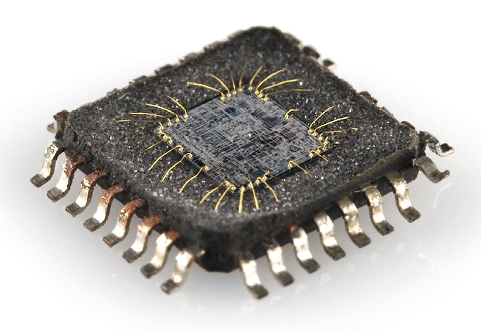
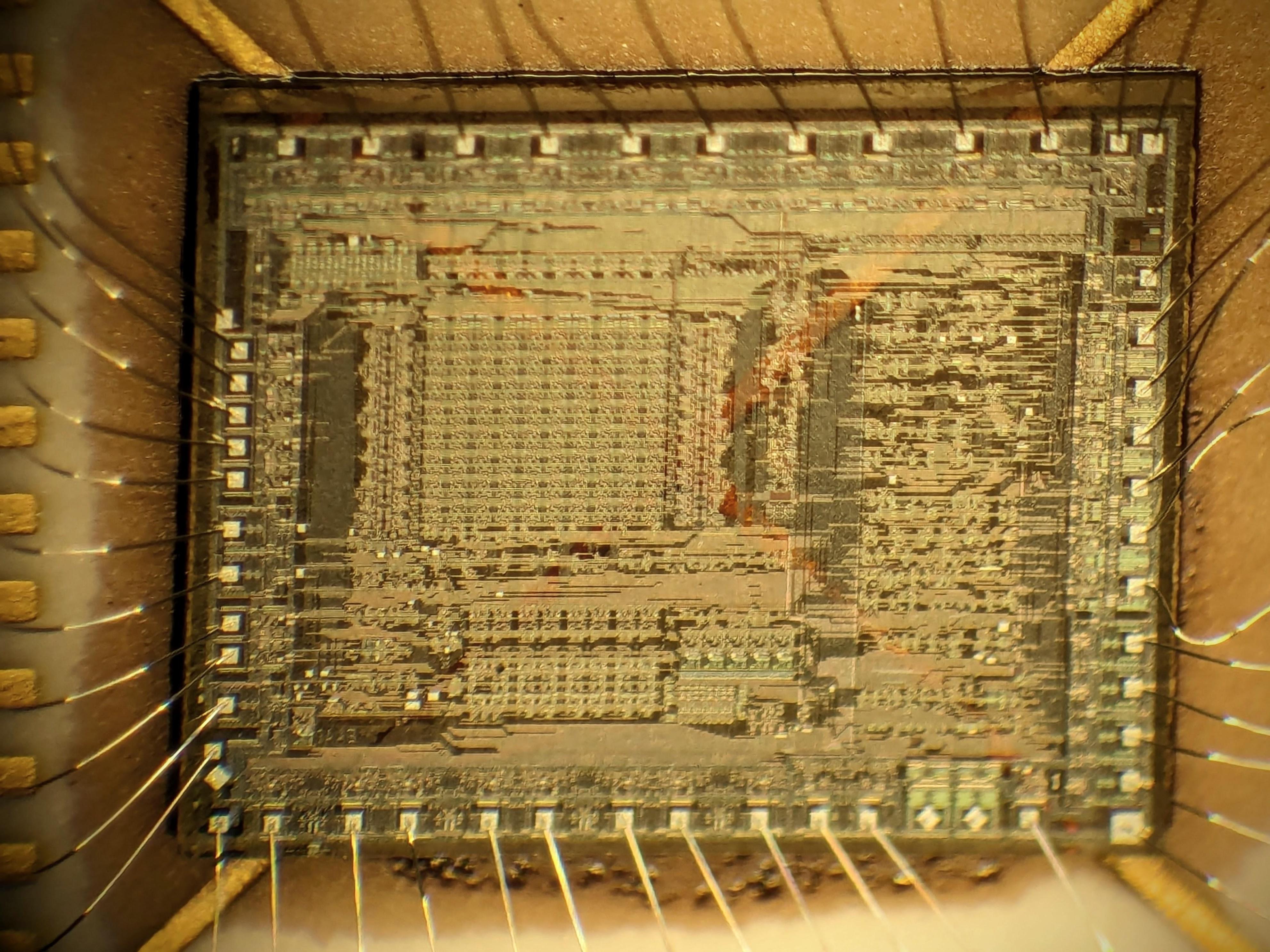
When a wafer is completed, it is cut into individual squares known as “dies.” Each die is a standalone chip. If you were to look at a die under an electron microscope, you wouldn’t see a flat surface; you would see a sprawling, multi-layered metropolis of switches and wires. The “process node”—measured in nanometers (nm)—refers to the size of the features on this die. Today’s cutting-edge chips, such as those produced by TSMC or Samsung, utilize 3nm and 5nm processes, where individual features are only dozens of atoms wide.
2. The Building Blocks: Transistors and Logic Gates
If a chip is a city, the transistors are the individual houses. A modern high-performance chip, like an Apple M-series or an NVIDIA H100 GPU, contains tens of billions of transistors. These are the fundamental units of computation.
The MOSFET: The World’s Most Important Switch
Most modern chips use a type of transistor called a MOSFET (Metal-Oxide-Semiconductor Field-Effect Transistor). Essentially, a transistor acts as a binary switch. It has three parts: a source, a drain, and a gate. When a small voltage is applied to the gate, it creates an electric field that allows current to flow from the source to the drain (the “ON” state or binary 1). When the voltage is removed, the current stops (the “OFF” state or binary 0).
In recent years, the industry has shifted to “FinFET” (Fin Field-Effect Transistor) designs, where the channel is raised into a 3D fin shape to provide better control over the electrical flow, reducing “leakage” as components get smaller and smaller.
Logic Gates and Boolean Algebra
Transistors do not work in isolation. They are wired together to form logic gates—AND, OR, NOT, and NAND. These gates are the physical manifestations of Boolean logic. For example, an AND gate only outputs a signal if both of its inputs are “ON.” By combining millions of these gates, engineers create functional units capable of addition, subtraction, and complex decision-making. This is the “brain” inside the chip: a massive, automated system of switches flipping billions of times per second.
3. Complex Architecture: Layers of Intelligence
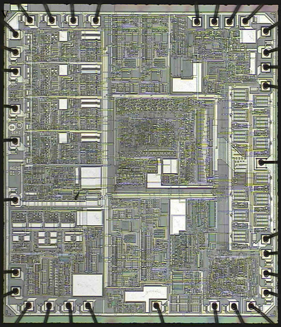
Looking inside a chip reveals a highly organized hierarchy. A chip is not just a random heap of transistors; it is structured into functional blocks, each with a specific purpose.
The Floorplan of a Chip
The layout of these blocks is called the “floorplan.” In a typical Central Processing Unit (CPU), you will find several key areas:
- The Control Unit: This acts as the conductor of the orchestra, directing the flow of data and instructions.
- ALU (Arithmetic Logic Unit): This is where the actual math happens. It handles integers and logical comparisons.
- Register Files: Small, ultra-fast storage areas that hold the data the ALU is currently working on.
Interconnects and the Metal Layers
While the transistors sit at the very bottom (the “front-end” of the line), the layers above them consist of a complex network of “interconnects.” These are microscopic wires, usually made of copper or cobalt, that connect the transistors to one another. A modern chip may have 10 to 15 layers of these metal wires stacked on top of each other. The bottom layers handle local connections between nearby transistors, while the upper layers handle “global” signals that carry data across the entire chip.
Packaging: Putting it All Together
What we see from the outside—the black square with gold pins—is actually the “package.” The silicon die itself is incredibly fragile. The package protects the die, provides the thermal cooling necessary to dissipate heat, and breaks out the microscopic connection points on the die to larger pins that can be soldered onto a motherboard.
4. Specialized Components within the Die
As the demand for specific types of computing grows, what is “inside” a chip has become more specialized. We have moved away from “monolithic” designs toward “Systems on a Chip” (SoC).
CPU vs. GPU vs. NPU
A modern smartphone chip is an SoC that contains several different types of processors:
- CPU: Optimized for “serial” processing—handling a variety of different tasks one after another.
- GPU (Graphics Processing Unit): Optimized for “parallel” processing. Inside a GPU, there are thousands of simpler cores designed to handle many mathematical operations simultaneously, which is essential for rendering video games or training AI.
- NPU (Neural Processing Unit): A relatively new addition to the chip’s interior. NPUs are hard-wired to perform the specific types of matrix multiplication used in artificial intelligence and machine learning, doing so with much higher efficiency than a general-purpose CPU.
Cache and Memory Controllers
Because the “main memory” (RAM) of a computer is physically far away from the chip, it is relatively slow. To solve this, chips include “Cache”—static RAM (SRAM) built directly into the silicon die. Level 1, Level 2, and Level 3 caches act as high-speed staging areas, keeping the most important data right next to the processing cores to prevent the transistors from sitting idle while waiting for information.
5. The Future of Chip Design: Beyond Traditional Limits
As we approach the physical limits of how small a transistor can be—atoms are only so small, after all—the “inside” of a chip is changing once again.
Chiplets and Heterogeneous Integration
Instead of trying to cram everything onto one massive, perfect piece of silicon (which is expensive and prone to defects), companies like AMD and Intel are moving toward “chiplets.” This involves breaking a large processor into smaller, specialized pieces (chiplets) and connecting them on a “bridge” or an interposer. Inside a chiplet-based processor, you might see components manufactured on different process nodes (e.g., a 5nm logic core connected to a 12nm I/O controller) all working as a single unit.
3D Stacking and Photonics
The next frontier is 3D ICs, where layers of logic and memory are stacked directly on top of each other, like a skyscraper. This drastically reduces the distance data has to travel, saving energy and increasing speed. Furthermore, researchers are looking at “silicon photonics”—using light (photons) instead of electricity (electrons) to move data within the chip, which would virtually eliminate the heat generated by traditional copper wiring.
Conclusion
When we ask “what is inside a chip,” the answer is a testament to human ingenuity. Inside that small sliver of silicon is a multi-dimensional lattice of billions of switches, a labyrinth of copper highways, and a masterfully planned architecture that operates at the speed of light. It is a world where distance is measured in atoms and time is measured in picoseconds. As we push toward the next generation of AI and quantum computing, the “city” inside the chip will only become more dense, more efficient, and more essential to every facet of our lives. Understanding this microscopic world is not just for engineers; it is for anyone who wishes to understand the infrastructure of the 21st century.
aViewFromTheCave is a participant in the Amazon Services LLC Associates Program, an affiliate advertising program designed to provide a means for sites to earn advertising fees by advertising and linking to Amazon.com. Amazon, the Amazon logo, AmazonSupply, and the AmazonSupply logo are trademarks of Amazon.com, Inc. or its affiliates. As an Amazon Associate we earn affiliate commissions from qualifying purchases.