
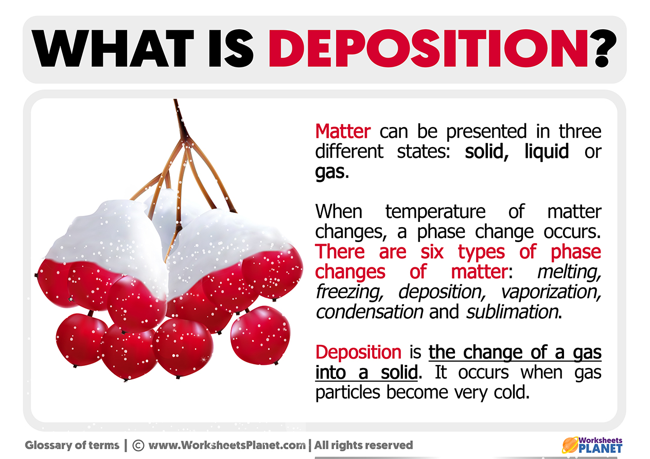
In the strictest scientific sense, deposition refers to the phase transition in which gas transforms directly into a solid without passing through the intermediate liquid phase. While meteorologists use the term to describe the formation of frost and geologists use it to explain the accumulation of sediment, the technology sector has adopted and refined this scientific principle to create the foundation of the modern digital world. From the microchips powering artificial intelligence to the high-resolution displays on our smartphones, deposition is the silent manufacturing powerhouse that enables the existence of high-tech hardware.
Understanding deposition in a technological context requires looking past the basic textbook definition and into the controlled environments of cleanrooms and vacuum chambers. In the tech industry, deposition is the process of applying thin films of material onto a substrate, such as a silicon wafer or a glass panel. These films can be as thin as a single atom, and they are essential for creating the complex circuits and sensors that drive our current technological landscape.
The Scientific Foundation of Deposition in Hardware Manufacturing
The science of deposition in technology is primarily concerned with the controlled growth of materials at the molecular or atomic level. Unlike traditional manufacturing, which often involves cutting or shaping bulk materials, tech-focused deposition is an additive process. It builds structures from the ground up, allowing for the extreme precision required for modern computing.
Thin-Film Physics and Substrate Interaction
In the realm of technology, the “science” of deposition revolves around the interaction between a source material and a substrate. The substrate acts as the canvas—usually a wafer of silicon or a sheet of specialized glass. Through various energetic processes, atoms of a coating material are “deposited” onto this canvas. The science here involves managing thermodynamics, kinetic energy, and surface chemistry to ensure that the atoms arrange themselves in a perfect crystalline structure or a uniform amorphous layer.
The Role of Vacuum Environments
To achieve the level of purity required for modern gadgets, deposition must occur in a vacuum. In the open air, oxygen and nitrogen molecules would interfere with the depositing atoms, leading to impurities that would ruin a semiconductor. By utilizing high-vacuum technology, scientists can ensure that only the intended materials reach the substrate. This scientific requirement has led to the development of some of the most advanced machinery in the world, including multi-million dollar deposition chambers used by global tech giants.
Chemical Vapor Deposition (CVD): The Architect of Modern Processors
When we discuss the “science” of how a CPU or GPU is made, we are largely talking about Chemical Vapor Deposition (CVD). This is the primary method used to grow the insulating and conducting layers that form the millions of transistors on a chip.
The Mechanism of Chemical Reaction
CVD involves placing a substrate in a reaction chamber and exposing it to one or more volatile precursors. These precursors react or decompose on the substrate surface to produce the desired thin-film deposit. Unlike physical methods, CVD relies on chemical affinity. This allows the material to “grow” even in deep trenches or around complex 3D structures on a chip, a property known as “conformal coverage.”
Impact on AI and High-Performance Computing
The rapid advancement of AI tools and large language models is directly tied to our ability to refine CVD processes. AI requires massive computational power, which in turn requires chips with higher transistor density. Advanced CVD techniques, such as Plasma-Enhanced Chemical Vapor Deposition (PECVD), allow manufacturers to create these layers at lower temperatures, preserving the integrity of the delicate circuits underneath. Without the scientific evolution of CVD, the hardware necessary to run modern AI software simply would not exist.
Variants: Low-Pressure and Metal-Organic CVD
The tech industry uses specific branches of CVD for different applications. Low-Pressure CVD (LPCVD) is often used for high-quality polycrystalline silicon, while Metal-Organic CVD (MOCVD) is the gold standard for creating LEDs and power electronics. Each of these represents a marriage of chemical engineering and hardware design, proving that the scientific meaning of deposition is central to every screen we look at and every server we access.
Physical Vapor Deposition (PVD): Protecting and Enhancing Hardware

While CVD is the heavy lifter for internal circuitry, Physical Vapor Deposition (PVD) is the technology of choice for creating the durable, functional surfaces of our gadgets and the metal interconnects that link components.
Sputtering and Evaporation Techniques
PVD is a purely physical process. In a PVD chamber, a solid source material is converted into a vapor through mechanical or thermal means—such as hitting it with high-energy ions (sputtering) or heating it with an electron beam (evaporation). This vapor then travels through the vacuum and condenses on the target gadget or component.
Enhancing Consumer Electronics
If you have ever wondered why a premium smartphone screen is so resistant to glare or why the casing of a luxury smartwatch doesn’t scratch easily, the answer lies in PVD. Tech companies use PVD to deposit thin layers of titanium nitride or chromium to provide hardness and aesthetic finishes. Furthermore, PVD is used to deposit the conductive copper or aluminum lines that act as the “wires” on a microchip, facilitating the high-speed data transfer required for modern digital security and high-speed internet.
The Role of PVD in Optical Technology
In the world of cameras and sensors, PVD is used to create anti-reflective coatings. This scientific application allows more light to reach the sensor, resulting in the high-quality photos we expect from modern mobile devices. By depositing layers of specific thickness, engineers can use the science of wave interference to cancel out reflections, a feat of tech-science that occurs at the nanometer scale.
Deposition in Additive Manufacturing: The Logic of 3D Printing
The term deposition also holds a vital place in the world of 3D printing and rapid prototyping, specifically through a process known as Fused Deposition Modeling (FDM).
Fused Deposition Modeling (FDM)
FDM is the most common form of 3D printing used by tech enthusiasts and professional engineers alike. In this context, “deposition” refers to the controlled extrusion of molten thermoplastic through a nozzle. The software translates a digital 3D model into a set of coordinates, and the printer deposits the material layer by layer to build a physical object. This is a direct application of the science of phase transitions—moving from a solid filament to a liquid state and back to a solid upon deposition.
Professional Applications and Prototyping
Beyond hobbyist use, deposition technology in 3D printing has revolutionized how tech hardware is prototyped. Instead of waiting weeks for a factory to mold a prototype, engineers use deposition-based printing to iterate designs in hours. In the aerospace and defense sectors, Direct Energy Deposition (DED) is used to repair high-end components by “depositing” metal powder and melting it with a laser, showcasing the high-stakes utility of this scientific process.
Atomic Layer Deposition (ALD) and the Future of Nano-Tech
As we push toward the physical limits of silicon, a specialized form of deposition called Atomic Layer Deposition (ALD) has become the most critical frontier in technology.
The Precision of Single Atom Layers
ALD is a subclass of CVD that allows for the growth of films one atomic layer at a time. It uses a self-limiting chemical reaction; the first precursor is pulsed into the chamber and coats the substrate in a single layer, then the second precursor is pulsed to react with the first. This creates a film with unparalleled thickness control and uniformity.
Enabling the Next Generation of AI and IoT
The move toward 3-nanometer and 2-nanometer chip architectures is only possible because of ALD. As components get smaller, the “science of deposition” becomes a game of counting individual atoms. This precision is what will enable the next generation of Internet of Things (IoT) devices, which require ultra-low power consumption and extremely small form factors.
Security and Integrity at the Atomic Level
Finally, deposition science plays a burgeoning role in digital security. Researchers are exploring the use of unique deposition patterns to create Physical Unclonable Functions (PUFs). These are hardware-level security keys that are nearly impossible to duplicate because they rely on the microscopic, random variations that occur during the deposition process. In an age of increasing cyber threats, the very way we deposit atoms on a chip may become our ultimate defense against hardware hacking and counterfeiting.
In conclusion, while the scientific definition of deposition may start in a chemistry or geology textbook, its most impactful application today is in the tech industry. It is the bridge between digital logic and physical reality, turning gases and vapors into the solid-state hardware that defines our modern existence. Understanding this process is key to understanding the trajectory of all future technology, from the devices in our pockets to the massive AI arrays in the cloud.
aViewFromTheCave is a participant in the Amazon Services LLC Associates Program, an affiliate advertising program designed to provide a means for sites to earn advertising fees by advertising and linking to Amazon.com. Amazon, the Amazon logo, AmazonSupply, and the AmazonSupply logo are trademarks of Amazon.com, Inc. or its affiliates. As an Amazon Associate we earn affiliate commissions from qualifying purchases.