
The transition toward a sustainable digital and physical infrastructure has placed photovoltaic (PV) technology at the forefront of the global energy revolution. As we move away from fossil fuels, the “gadgets” powering our homes and data centers have shifted from combustion engines to sophisticated semiconductor devices. To understand the efficiency, durability, and future trajectory of solar energy, one must look closely at the material science that makes it possible.
A photovoltaic panel is not a single piece of equipment but a complex assembly of high-tech materials designed to facilitate the “photovoltaic effect.” This process involves converting light (photons) directly into electricity (voltage) at the atomic level. This article explores the intricate components that comprise modern solar panels, from the primary semiconductors to the protective layers that ensure a 25-year lifespan.
The Heart of the Tech: Silicon and Semiconductor Layers
At the core of approximately 95% of solar panels sold today is silicon. Silicon is a semiconductor, meaning it has electrical conductivity properties between that of a conductor (like copper) and an insulator (like glass). In the tech world, silicon is the foundation of the microchips in our smartphones and computers; in the energy world, it is the engine of the solar cell.
Monocrystalline vs. Polycrystalline Silicon
The performance of a solar panel is largely determined by the purity and structure of its silicon.
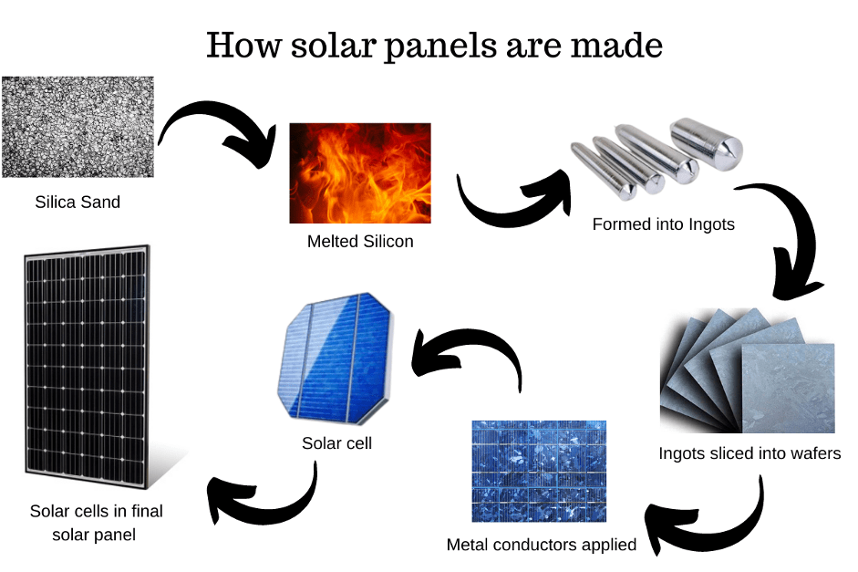
- Monocrystalline Silicon: These cells are made from a single, continuous crystal structure. Using the Czochralski process, a seed crystal is dipped into molten silicon and slowly withdrawn to create a cylindrical ingot. This ingot is then sliced into wafers. Because the crystals are highly pure and aligned, electrons have more room to move, resulting in higher efficiency ratings (often exceeding 22%).
- Polycrystalline Silicon: Instead of a single crystal, these cells are made by melting fragments of silicon together. This results in a “mosaic” look. While cheaper to manufacture, the boundaries between the crystals act as barriers to electron flow, making these panels slightly less efficient than their monocrystalline counterparts.
Doping and the P-N Junction
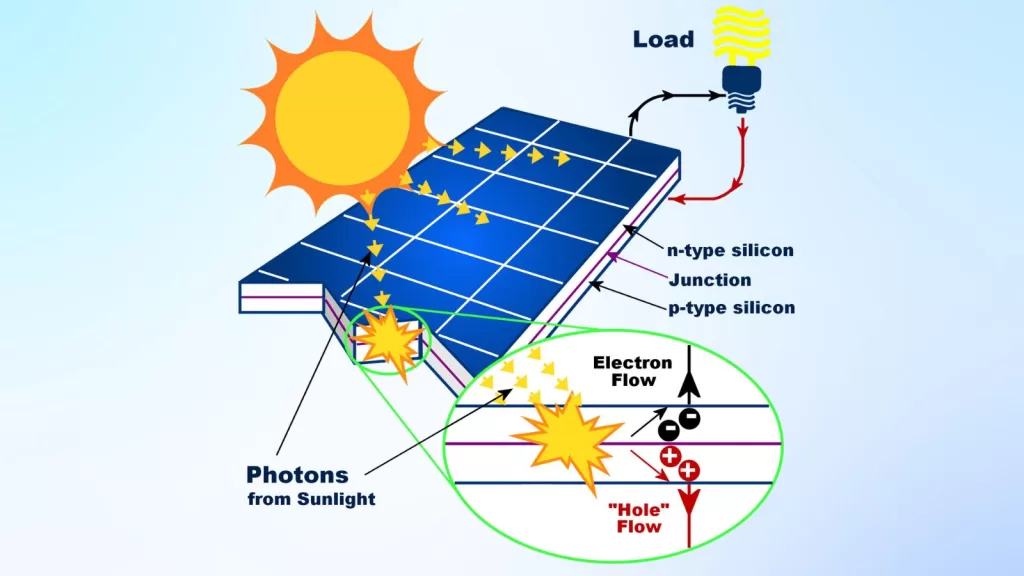
Raw silicon is not a great conductor on its own. To make it functional for energy production, engineers use a process called “doping.” The silicon wafer is treated with impurities to create two distinct layers:
- N-type (Negative): Silicon is infused with phosphorus, which has five electrons in its outer shell (one more than silicon). This creates an abundance of “free” electrons.
- P-type (Positive): Silicon is infused with boron, which has three electrons, creating “holes” where an electron should be.
When these two layers are sandwiched together, they create a P-N junction. This junction establishes an internal electric field that acts as a gatekeeper, forcing electrons knocked loose by sunlight to flow in a specific direction, thereby creating an electric current.
Beyond Silicon: Thin-Film and Emerging Material Technologies
While crystalline silicon dominates the market, the tech industry is constantly iterating on alternative materials that offer flexibility, lower weight, or different absorption spectrums. These are broadly categorized as “Thin-Film” technologies.
Cadmium Telluride (CdTe) and CIGS
Thin-film panels are created by depositing one or more layers of photovoltaic material onto a substrate, such as glass, plastic, or metal.
- Cadmium Telluride (CdTe): This is the most common thin-film tech. It uses a layer of cadmium telluride to capture sunlight. While it has a lower efficiency than silicon, it is cheaper to manufacture at scale and performs better in high-temperature environments.
- Copper Indium Gallium Selenide (CIGS): These cells offer higher efficiency among thin-films. Because the material can be deposited on flexible surfaces, CIGS is the “gadget” of choice for portable solar chargers and integrated solar fabrics.
The Perovskite Revolution
Perhaps the most exciting trend in solar tech today is the development of Perovskites. These are a class of compounds characterized by a specific crystallographic structure. Perovskites are lightweight, flexible, and—most importantly—can be manufactured using simple chemical “printing” techniques rather than high-heat industrial processes.
In the tech lab, researchers are currently focused on “Tandem Cells,” which layer Perovskite on top of traditional silicon. This allows the panel to capture different wavelengths of the light spectrum, pushing efficiency limits toward 30%, a feat previously thought impossible for commercial hardware.
Structural Components: The Anatomy of a Solar Module
A solar cell by itself is incredibly fragile, often no thicker than a human hair. To function in the real world—facing hail, wind, and extreme UV exposure—it must be integrated into a ruggedized module.
Tempered Glass and Anti-Reflective Coatings
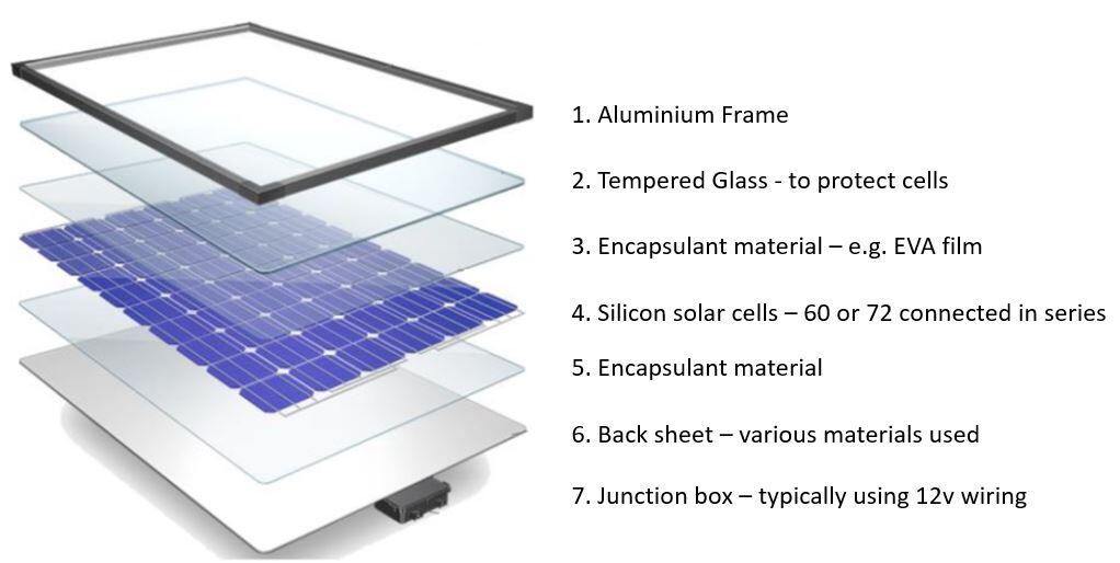
The front-facing surface of a solar panel is high-transmittance tempered glass. This isn’t ordinary window glass; it is designed to be “low-iron,” which increases clarity and allows more photons to reach the silicon.
Furthermore, the glass is treated with an anti-reflective (AR) coating. Without this tech, a significant portion of sunlight would bounce off the panel and back into the atmosphere. The AR coating ensures that the maximum amount of light is absorbed into the semiconductor layers.
The Encapsulant: Ethylene Vinyl Acetate (EVA)
To protect the silicon cells from moisture and mechanical shock, they are “potted” or encapsulated. The industry standard is Ethylene Vinyl Acetate (EVA). This is a thin layer of polymer that, when heated during the manufacturing process, creates a waterproof seal around the cells. High-quality EVA is crucial because if it degrades or “yellows” over time, it will block light and reduce the panel’s output.
Backsheets and Frames
The back of the panel is typically covered by a “backsheet,” a multilayer polymer film (often involving Tedlar). Its job is to provide electrical insulation and protect the internal components from the elements.
The entire “sandwich” (glass, EVA, cells, backsheet) is then encased in an anodized aluminum frame. Aluminum is chosen for its high strength-to-weight ratio and its natural resistance to corrosion, ensuring the panel remains structurally sound for decades.
Conducting the Current: Metalization and The Junction Box
Once the photons have displaced electrons in the silicon, the energy needs a “highway” to exit the panel and enter the power grid or your home’s battery system.
Silver and Aluminum Contacts
On the surface of the silicon wafers, you will see a grid of fine lines. These are “fingers” and “busbars,” usually made of silver paste. Silver is the most conductive metal on earth, making it ideal for collecting electrons. However, because silver is expensive, a major tech trend in solar manufacturing is “metalization optimization”—using thinner silver lines or substituting them with copper to lower costs without sacrificing conductivity.
The Junction Box and Bypass Diodes
On the back of the panel sits the junction box. This is the “brain” of the panel’s external interface. Inside, you will find bypass diodes. These are critical digital components that prevent the panel from failing if one section is shaded. If a leaf covers part of the panel, the bypass diode allows the current to “skip” that section, ensuring the rest of the panel continues to produce power efficiently.
The Future of PV Materials: Efficiency and Sustainability
As we look toward the next generation of solar tech, the focus is shifting from simple power generation to lifecycle sustainability and resource management.
Reducing Rare Mineral Dependency
The tech industry is keenly aware of the supply chain risks associated with rare minerals. Current R&D is focused on reducing the amount of silver and lead used in panels. Some manufacturers are experimenting with “lead-free” perovskites and graphene-based conductive inks to replace precious metals.
The Circular Tech Economy: Recycling
The question of what happens at the end of a panel’s life is a major topic in green tech. Modern panels are nearly 90% recyclable by weight. The glass and aluminum are easily reclaimed, but the challenge lies in the “delamination” process—separating the silicon and silver from the EVA plastic. Advanced thermal and chemical recycling plants are now coming online, treated much like e-waste facilities, to ensure that the materials in today’s panels become the raw components for tomorrow’s energy solutions.
Conclusion
A photovoltaic panel is a masterpiece of modern engineering, bridging the gap between basic chemistry and advanced electronics. From the precise “doping” of silicon crystals to the protective polymers and anti-reflective coatings, every material is chosen for its ability to handle photons and electrons with maximum efficiency. As thin-film and perovskite technologies continue to mature, we are moving toward a world where solar tech is not just on our roofs, but integrated into our windows, our clothing, and our mobile devices, marking a new era of ubiquitous, material-driven energy.
aViewFromTheCave is a participant in the Amazon Services LLC Associates Program, an affiliate advertising program designed to provide a means for sites to earn advertising fees by advertising and linking to Amazon.com. Amazon, the Amazon logo, AmazonSupply, and the AmazonSupply logo are trademarks of Amazon.com, Inc. or its affiliates. As an Amazon Associate we earn affiliate commissions from qualifying purchases.