
In the rapidly evolving landscape of technology, the term “conduction” often sits quietly in the background, overshadowed by flashy buzzwords like Artificial Intelligence, Blockchain, or Quantum Computing. However, conduction is the fundamental physical process that makes every piece of modern hardware possible. Whether we are discussing the movement of electrons through a microscopic circuit or the dissipation of heat from a high-performance server, conduction is the silent engine of the digital age.
To understand conduction in a tech context is to understand the lifeblood of our devices. It is the bridge between raw energy and functional processing. As we push the boundaries of transistor density and processing speed, the mastery of both electrical and thermal conduction has become the primary bottleneck—and the primary opportunity—for innovation in the tech industry.
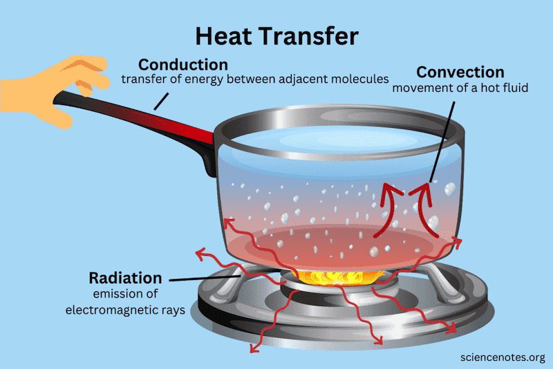
Understanding the Fundamentals: Electrical and Thermal Conduction in Hardware
At its core, conduction is the transfer of energy through a medium without the overall motion of the medium itself. In the realm of technology, this manifests in two distinct but inextricably linked forms: electrical conduction and thermal conduction.
The Atomic Level of Connectivity
Electrical conduction occurs when a potential difference (voltage) is applied across a conductor, causing charge carriers—typically electrons—to flow. In the hardware world, copper and gold are the gold standards for this process. Copper is favored for its high conductivity-to-cost ratio, appearing in everything from PCB traces to power cables. Gold, while more expensive, is used in connectors and bond wires due to its exceptional resistance to corrosion, ensuring that the conductive path remains uninterrupted over years of use.
The efficiency of this conduction determines the power consumption and speed of a device. Every bit of resistance encountered during electrical conduction results in energy loss, usually converted into heat. This leads us to the second, and arguably more challenging, form of conduction in modern tech.
Semiconductors and the Control of Flow
The true genius of modern electronics lies in the semiconductor. Materials like silicon do not conduct electricity as freely as metals, but their conductive properties can be precisely manipulated through a process called doping. By adding impurities, engineers can create regions that are more or less conductive, forming the basis of transistors.
The “on” and “off” states of a transistor are essentially high-conduction and low-conduction states. As we shrink these transistors down to the 3nm and 2nm nodes, managing how electrons move through these incredibly small spaces becomes a matter of quantum physics. At these scales, leakage—where electrons “jump” or conduct when they aren’t supposed to—becomes a major hurdle for chip designers like TSMC, Intel, and NVIDIA.
Thermal Conduction: The Silent Guardian of High-Performance Computing
As processors become more powerful, they generate an immense amount of heat. This is a direct byproduct of electrical resistance during conduction. If this heat isn’t moved away from the silicon die quickly, the chip will “thermal throttle,” reducing its performance to prevent physical damage. This is where thermal conduction becomes the most critical factor in hardware design.
Heat Sinks and Thermal Interface Materials (TIMs)
Thermal conduction is the process by which heat energy moves from a hot object to a cooler one through direct contact. In a computer, this journey begins at the surface of the CPU or GPU. To facilitate this, engineers use Thermal Interface Materials (TIMs), such as thermal paste or liquid metal. These materials are designed to fill the microscopic air gaps between the processor and the cooling solution, as air is a poor conductor of heat.
Once the heat passes through the TIM, it enters a heat sink, usually made of aluminum or copper. Copper is the preferred choice for the baseplate because its thermal conductivity is significantly higher than that of aluminum. The goal is to move the heat away from the sensitive silicon as efficiently as possible, relying on the high conductive capacity of these metals.
The Impact of Conduction on Longevity and Stability
The effectiveness of a device’s thermal conduction directly impacts its lifespan. Consistent exposure to high temperatures can lead to a phenomenon known as electromigration, where the atoms in the metal traces of a chip are slowly pushed out of place by the flow of electrons. This eventually leads to circuit failure.
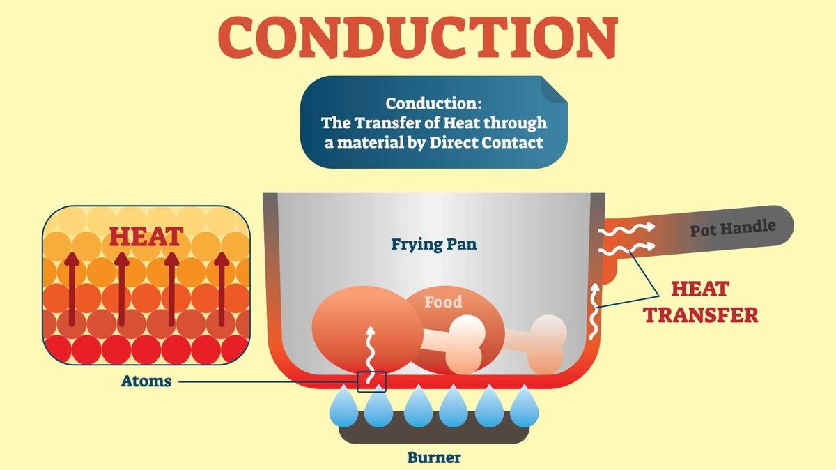
By optimizing thermal conduction, manufacturers can ensure that devices run cooler, last longer, and maintain peak performance levels. This is why we see increasingly complex cooling solutions in modern gadgets, from the massive triple-fan arrays on modern graphics cards to the sophisticated vapor chambers found in high-end smartphones.
Innovations in Material Science: Enhancing Conduction for Next-Gen Devices
We are reaching the physical limits of traditional materials like silicon and copper. To continue the trajectory of Moore’s Law, the tech industry is turning to material science to find new ways to enhance conduction.
Graphene and Two-Dimensional Materials
Graphene is often hailed as a “wonder material” in the tech world due to its extraordinary conductive properties. It is a single layer of carbon atoms arranged in a hexagonal lattice, and it conducts electricity and heat with far greater efficiency than copper or silicon.
In the world of electrical conduction, graphene-based transistors could theoretically operate at much higher frequencies while consuming less power. In the realm of thermal conduction, graphene sheets are already being used in smartphones to spread heat away from the battery and processor, preventing hotspots and improving the user experience during intensive tasks like gaming or 4K video recording.
Liquid Cooling and Advanced Substrates
While not a “material” in the traditional sense, the move toward liquid cooling in data centers and enthusiast PCs is a shift in how we utilize conduction. Direct-to-chip liquid cooling uses a conductive cold plate to transfer heat to a circulating liquid. Furthermore, the industry is exploring Gallium Nitride (GaN) as a replacement for silicon in power electronics. GaN has a wider bandgap, allowing it to conduct electricity at much higher voltages and temperatures with less resistance, which is why modern “fast chargers” can be so much smaller and more efficient than their predecessors.
Conduction in the Era of AI and Edge Computing
The rise of Artificial Intelligence (AI) has placed an unprecedented strain on conductive systems. AI workloads, particularly the training of Large Language Models (LLMs), require massive clusters of GPUs working in parallel. This creates a density of heat and power demand that traditional infrastructure was never designed to handle.
Managing the Thermal Density of Data Centers
In a modern data center housing thousands of H100 GPUs, conduction is the primary design constraint. Engineers must calculate the thermal conductivity of every component to ensure that the heat generated by these chips can be moved out of the rack and eventually out of the building. This has led to the rise of immersion cooling, where entire servers are submerged in non-conductive (dielectric) fluids. In this setup, the fluid is in direct contact with every component, maximizing the surface area for thermal conduction.
Power Efficiency through Superior Conductive Design
For edge computing—where AI processing happens on the device rather than in the cloud—efficiency is king. Devices like the Apple Silicon chips (M-series) or Qualcomm’s Snapdragon platforms succeed because they optimize the conductive paths within the SoC (System on a Chip). By placing memory closer to the processing cores, they reduce the distance electrons must travel, minimizing the energy lost to resistance and maximizing the speed of data conduction.

The Future of Conductive Engineering
As we look toward the future, the “what” of conduction remains the same, but the “how” is changing drastically. We are moving toward a world where conduction is managed at the molecular level.
Optical computing, for instance, seeks to replace electrical conduction with the “conduction” of photons through fiber optics on a chip level. Photons generate virtually no heat compared to electrons, potentially solving the thermal conduction problem entirely. However, until such technologies become commercially viable, the tech industry will continue to rely on the mastery of traditional conduction.
In conclusion, conduction is far more than a basic physics concept; it is the fundamental challenge of modern hardware engineering. From the microscopic traces on a smartphone motherboard to the massive cooling arrays in an AI data center, the ability to move electrons and heat efficiently is what separates cutting-edge technology from obsolete hardware. As we demand more power, more speed, and more intelligence from our devices, our understanding and application of conduction will remain the most critical factor in the next generation of technological breakthroughs.
aViewFromTheCave is a participant in the Amazon Services LLC Associates Program, an affiliate advertising program designed to provide a means for sites to earn advertising fees by advertising and linking to Amazon.com. Amazon, the Amazon logo, AmazonSupply, and the AmazonSupply logo are trademarks of Amazon.com, Inc. or its affiliates. As an Amazon Associate we earn affiliate commissions from qualifying purchases.