
For more than half a century, Intel Corporation has been synonymous with the evolution of the modern computer. While the “Intel Inside” stickers found on millions of laptops and desktops are a global branding phenomenon, the physical engine driving this technological revolution is located in a specific corner of Northern California. Intel is headquartered in Santa Clara, California, at the Robert Noyce Building. This location is not merely a corporate mailing address; it is the spiritual and operational epicenter of Silicon Valley, the region Intel helped name and define.
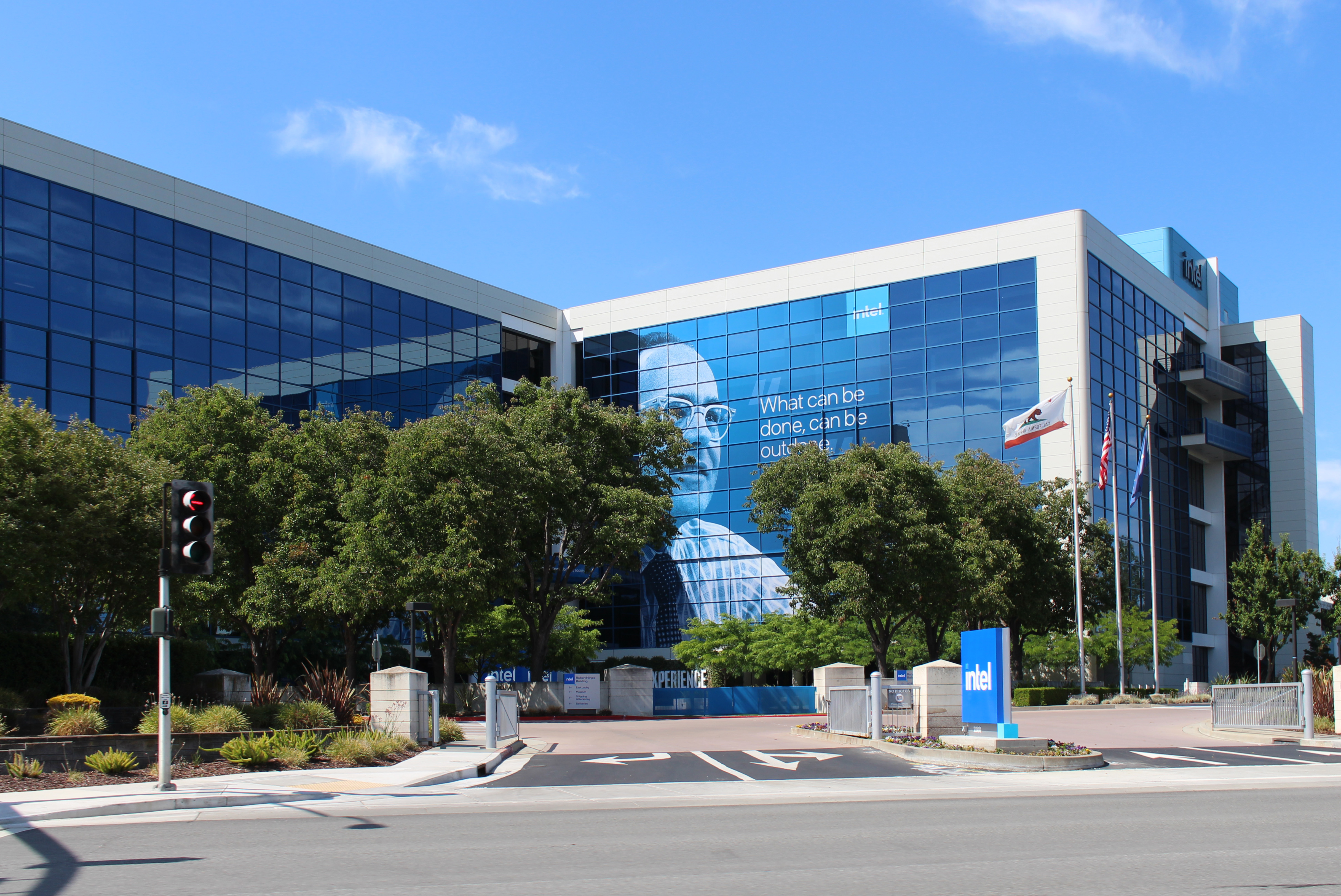
Understanding where Intel is headquartered requires more than just a pin on a map. It involves exploring a massive global infrastructure that spans from the R&D labs of Oregon to the high-tech fabrication plants (fabs) of Arizona, Ireland, and Israel. However, the Santa Clara campus remains the brain of the operation, where executive strategy, core architecture design, and the future of the semiconductor industry are shaped.
The Robert Noyce Building: The Epicenter of Silicon Valley
The primary headquarters of Intel sits at 2200 Mission College Boulevard in Santa Clara. Named after the legendary co-founder Robert Noyce—often referred to as the “Mayor of Silicon Valley”—this facility serves as the nerve center for a company that powers the vast majority of the world’s data centers and personal computers.
A Legacy of Innovation in Santa Clara
When Robert Noyce and Gordon Moore left Fairchild Semiconductor to start Intel in 1968, they chose the Santa Clara Valley because of its burgeoning ecosystem of engineering talent and proximity to research institutions like Stanford University. At the time, the area was still characterized by fruit orchards. Intel’s arrival and subsequent success were pivotal in transforming the region into the global tech powerhouse it is today.
The Robert Noyce Building is more than an office space; it is a monument to the microprocessor. It houses the Intel Museum, a 10,000-square-foot facility that invites visitors and employees alike to explore the history of the integrated circuit. For tech enthusiasts, the museum provides an inside look at how silicon is transformed into the complex processors that drive AI, cloud computing, and gaming.
The Culture of the “Intel Cubicle”
Intel’s headquarters also became famous for its unique corporate culture. Unlike many of its contemporaries in the 1970s and 80s that maintained rigid hierarchies, Intel pioneered an egalitarian office layout. Even the highest-level executives, including former CEOs like Andy Grove, worked in open-plan cubicles. This design was intended to facilitate rapid communication and technical collaboration—essential traits in an industry where Moore’s Law dictates that the number of transistors on a chip doubles roughly every two years. Today, while the interiors have been modernized to support hybrid work and high-tech collaboration, that spirit of engineering-first transparency remains a core part of the Santa Clara identity.
Beyond Santa Clara: The Technical Powerhouse of Hillsboro, Oregon
While Santa Clara is the official headquarters for executive and administrative functions, the true “technical headquarters” of Intel’s research and development is arguably located in Hillsboro, Oregon. Known as the “Silicon Forest,” the Oregon campus is where Intel’s most advanced process technologies are developed before being exported to factories around the world.
Ronler Acres and the D1X Fab
The Ronler Acres campus in Hillsboro is perhaps the most technologically advanced site in the Intel network. It is home to the D1X factory, a massive research and development facility where engineers work on the “next node” of semiconductor manufacturing. In the world of high-tech hardware, a “node” refers to the specific generation of manufacturing technology (such as Intel 4 or Intel 18A).
In Oregon, Intel’s engineers grapple with the physics of the incredibly small. They utilize Extreme Ultraviolet (EUV) lithography machines—devices roughly the size of a city bus that use light of an incredibly short wavelength to “print” transistor patterns onto silicon wafers. The work done in Hillsboro is what allows Intel to maintain its competitive edge in the high-stakes race for transistor density and energy efficiency.

Scaling Innovation Globaly
The relationship between the Santa Clara HQ and the Oregon R&D hub is a symbiotic one. Santa Clara sets the product roadmap—deciding, for example, that the next generation of processors must prioritize AI acceleration—while the Oregon teams figure out the physical and chemical engineering required to make those designs a reality. This multi-billion-dollar feedback loop is what has enabled Intel to survive decades of technological shifts, from the transition to mobile computing to the current explosion of generative AI.
The Global Manufacturing Web: Arizona, Ireland, and Israel
Intel’s footprint extends far beyond the United States, reflecting the globalized nature of modern technology. To support the designs coming out of Santa Clara and the processes perfected in Oregon, Intel operates a massive network of high-volume manufacturing facilities.
The Ocotillo Campus in Arizona
The Ocotillo campus in Chandler, Arizona, is one of Intel’s most significant production hubs. Here, the company operates several massive fabs that churn out millions of chips every year. Arizona is currently the focus of Intel’s “IDM 2.0” strategy, a bold plan under CEO Pat Gelsinger to regain undisputed leadership in chip manufacturing. This includes a massive multi-billion-dollar investment to build new fabs that will not only produce Intel’s own chips but also serve as a “foundry” for other tech companies.
Ireland and the European Tech Gateway
In Leixlip, Ireland, Intel operates one of its most important European outposts. This site was the first to bring EUV technology to high-volume manufacturing in Europe. The Irish headquarters is critical for Intel’s presence in the European Union, serving as a hub for both manufacturing and design. It ensures that the company can navigate global supply chain challenges while tapping into the deep pool of engineering talent across the continent.
Israel: The Heart of Processor Architecture
Intel’s presence in Israel is legendary within the tech community. The Haifa design center has been responsible for some of the most significant breakthroughs in CPU architecture, including the “Centrino” mobile platform and the “Core” architecture that saved Intel from a performance slump in the mid-2000s. The Kiryat Gat manufacturing site in Israel is another pillar of the company’s global production, integrating cutting-edge manufacturing with world-class architectural design.
The New Frontier: Ohio and the Shift in Tech Geography
As the demand for domestic semiconductor manufacturing grows, Intel is expanding its headquarters philosophy to a new region: the “Silicon Heartland.” In 2022, Intel announced a massive investment in New Albany, Ohio, to build a new mega-site that could eventually become the largest semiconductor manufacturing location on the planet.
The Strategic Shift to the Midwest
The move to Ohio represents a significant shift in the geography of American technology. While Silicon Valley remains the brain, the Midwest is set to become the muscle. This new campus is designed to address the global chip shortage and reduce the industry’s heavy reliance on East Asian supply chains. For Intel, this site is not just another factory; it is a strategic expansion of their corporate footprint that aims to create a new ecosystem of suppliers and tech talent in the center of the United States.
Engineering the Future of AI and Beyond
The Ohio site will be critical for the production of chips using the Intel 18A process node. This technology is expected to introduce “PowerVia” (a new way of delivering power to the chip from the backside) and “RibbonFET” (a new transistor architecture). By placing these advanced technologies in a brand-new, massive-scale facility, Intel is betting that the future of tech leadership will be defined by whoever can most reliably manufacture at the “Angstrom era” level—where features are measured in fractions of a nanometer.

Conclusion: A Global Network Anchored in Santa Clara
While Intel’s operations are spread across the globe—from the rainy forests of Oregon to the deserts of Arizona and the tech hubs of Israel—the heart of the company remains firmly rooted in Santa Clara. The Robert Noyce Building stands as a reminder of where the digital age began and continues to serve as the guiding light for the company’s future.
In the fast-moving world of technology, Intel’s headquarters is more than just a place where people go to work. it is a symbol of the relentless pursuit of the “next big thing.” Whether it is the development of next-generation AI accelerators or the engineering of the world’s most advanced transistors, the decisions made at 2200 Mission College Boulevard will continue to ripple through every smartphone, laptop, and data center on the planet. As Intel navigates the complexities of the AI era and the challenges of modern manufacturing, its headquarters remains the epicenter of an industry that shows no signs of slowing down.
aViewFromTheCave is a participant in the Amazon Services LLC Associates Program, an affiliate advertising program designed to provide a means for sites to earn advertising fees by advertising and linking to Amazon.com. Amazon, the Amazon logo, AmazonSupply, and the AmazonSupply logo are trademarks of Amazon.com, Inc. or its affiliates. As an Amazon Associate we earn affiliate commissions from qualifying purchases.