
For over five decades, Advanced Micro Devices (AMD) has been a cornerstone of the computing world. While most consumers know AMD through the Ryzen processor in their laptop or the Radeon graphics card in their gaming rig, the physical reality of the company is a sprawling, multi-continental operation. Determining where AMD is “located” requires looking beyond a single corporate address to understand a complex web of research and development centers, executive hubs, and strategic manufacturing partnerships that span the globe.
In the high-stakes world of semiconductor technology, location is more than just a mailing address; it is a strategic asset. From the design laboratories of North America to the high-tech fabrication plants of East Asia, AMD’s physical presence dictates its ability to innovate, compete, and supply the world’s most critical technologies.

The Silicon Heart: Santa Clara and the Corporate Headquarters
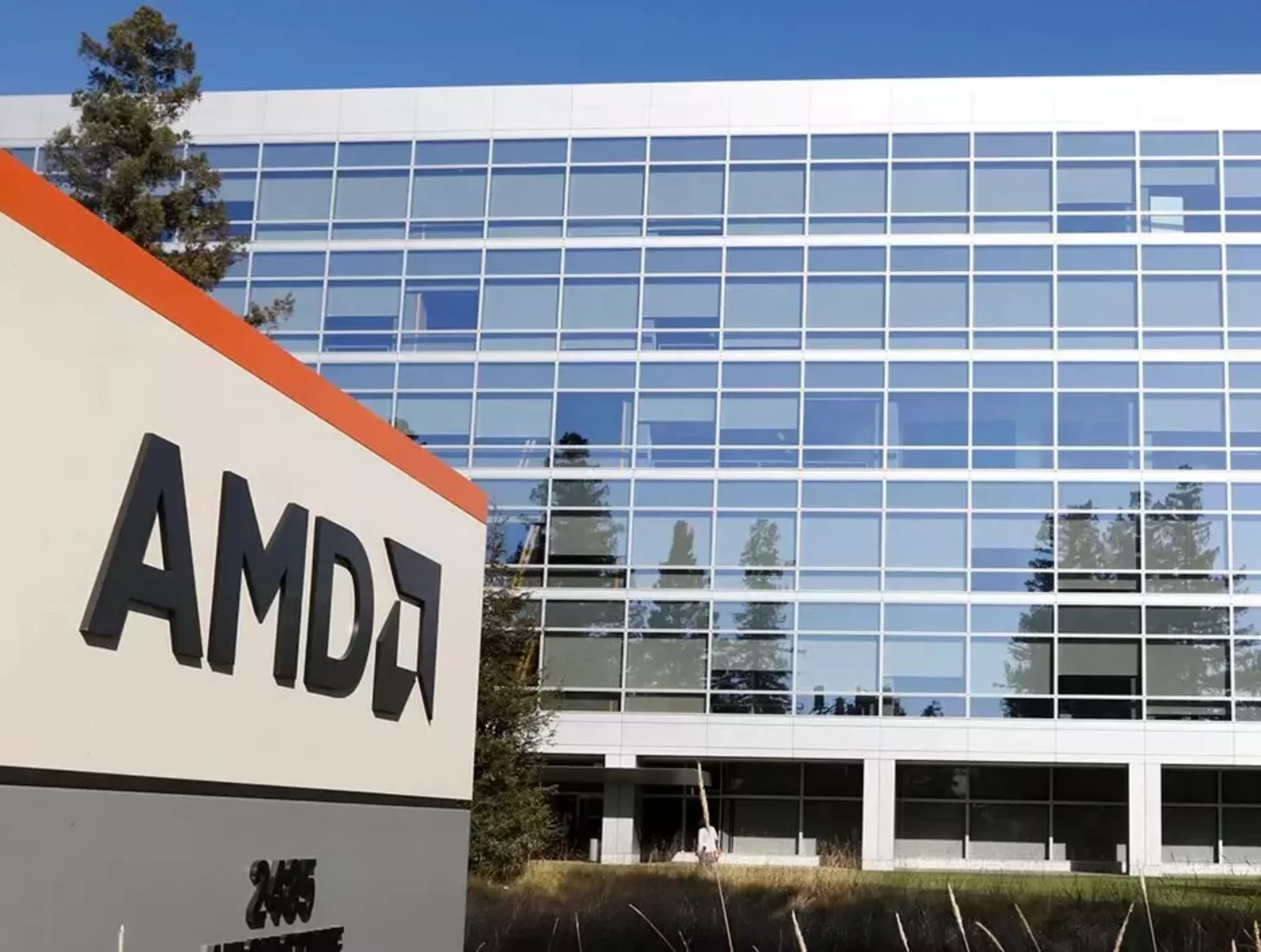
AMD’s primary identity is rooted in Silicon Valley. For much of its history, the company was synonymous with Sunnyvale, California. However, in recent years, AMD transitioned its global headquarters to a state-of-the-art facility in Santa Clara, placing it at the epicenter of the world’s most influential technology corridor.
The Transition to Santa Clara
The move to the 220,000-square-foot facility at 2485 Augustine Drive marked a symbolic and functional shift for the company. Located within the “Square” of Silicon Valley, this headquarters serves as the nerve center for AMD’s executive leadership, global marketing, and core administrative functions. The facility is designed for collaboration, reflecting the modern tech industry’s emphasis on open-concept workspaces and high-tech meeting environments. For AMD, being in Santa Clara isn’t just about prestige; it is about physical proximity to partners, competitors, and the deepest talent pool in the software and hardware engineering sectors.
Strategic Proximity to the Tech Ecosystem
Being located in Santa Clara puts AMD within a few miles of its primary rivals and closest collaborators. This geographical concentration facilitates the rapid exchange of ideas and the “agglomeration effect” that has made Silicon Valley the world’s premier tech hub. Whether it is collaborating with software developers to optimize drivers for a new architecture or engaging with cloud service providers to deploy EPYC server chips, the Santa Clara headquarters acts as the diplomatic and strategic gateway for all AMD operations.
A Distributed R&D Network: Where Innovation Happens
While Santa Clara houses the leadership, the actual “magic”—the architectural design of CPUs and GPUs—takes place in dedicated research and development (R&D) hubs spread across North America and the world. AMD’s “location” is effectively decentralized, with specific regions specializing in different aspects of the silicon lifecycle.
The Austin Powerhouse: Designing the Zen Architecture
If Santa Clara is the brain, Austin, Texas, is the engine room. AMD’s Austin campus is one of its largest and most critical sites. Historically, Austin has been the birthplace of many of AMD’s most successful CPU architectures, including the transformative “Zen” architecture that returned AMD to a position of dominance in the desktop and server markets.
The Austin facility is home to thousands of engineers specializing in microprocessor design, system-on-chip (SoC) integration, and software validation. The Texas location is vital for AMD’s recruitment strategy, tapping into the “Silicon Hills” ecosystem and the steady stream of engineering talent from regional universities.
Markham and the ATI Legacy: Driving GPU Excellence
When AMD acquired the Canadian company ATI Technologies in 2006, it inherited a massive R&D footprint in Markham, Ontario. Today, the Markham site remains the primary hub for AMD’s graphics technology development. This location is where the Radeon RDNA architectures are refined. The Canadian team provides the essential link between hardware design and the software stacks required for modern gaming, professional visualization, and AI acceleration.
Global Engineering Hubs: India and Beyond
AMD’s R&D footprint extends deep into Asia, particularly in India. With major design centers in Bangalore and Hyderabad, AMD leverages a massive workforce dedicated to hardware design, verification, and software development. In late 2023, AMD announced the opening of its largest global design center in Bangalore, the “Technostar” campus. This facility underscores AMD’s commitment to a globalized engineering model, ensuring that the sun never sets on the development of its next-generation silicon.
The “Fabless” Reality: Where AMD Chips Are Actually Made
Perhaps the most important distinction in understanding where AMD is located is the “fabless” business model. Unlike its long-time rival Intel, which manufactures many of its own chips in-house, AMD spun off its manufacturing arm (which became GlobalFoundries) in 2009. Today, AMD designs the chips, but the physical location of their “birth” is in the world’s most advanced third-party foundries.
The Strategic Partnership with TSMC in Taiwan
The vast majority of AMD’s cutting-edge products—including the Ryzen 7000 and 9000 series, EPYC server processors, and Radeon GPUs—are physically manufactured in Taiwan by the Taiwan Semiconductor Manufacturing Company (TSMC).
When we ask where AMD’s technology is located, the answer is often the high-tech industrial parks of Hsinchu and Tainan. TSMC’s state-of-the-art “GigaFabs” use extreme ultraviolet (EUV) lithography to print AMD’s designs onto silicon wafers at the 5nm, 4nm, and 3nm nodes. This geographical reliance on Taiwan is a critical component of AMD’s technological edge, as TSMC currently leads the world in transistor density and power efficiency.
Legacy Ties and GlobalFoundries
While TSMC handles the high-performance logic, AMD still utilizes GlobalFoundries for certain components. GlobalFoundries has a significant physical presence in Malta, New York, and Dresden, Germany. Some of the I/O (Input/Output) dies used in AMD’s chiplet-based designs are produced in these facilities. This multi-foundry approach means that a single AMD processor might contain silicon “located” and manufactured in both Taiwan and the United States before being assembled.
Assembly, Testing, and Packaging (ATP)
Once the silicon wafers are printed, they must be cut, tested, and packaged into the final products that consumers buy. AMD’s supply chain locations for ATP are primarily concentrated in Southeast Asia. Facilities in Malaysia (Penang) and China (Suzhou) play a vital role in the final stages of the production process. These locations are responsible for the meticulous work of mounting the silicon dies onto substrates, attaching heat spreaders, and conducting the final quality control tests that ensure a processor can hit its rated clock speeds.
Scaling the AI Frontier: The Impact of the Xilinx Integration
The acquisition of Xilinx in 2022 significantly expanded AMD’s physical and technological map. Xilinx, the leader in field-programmable gate arrays (FPGAs) and adaptive computing, brought with it a massive headquarters in San Jose, California, and a global network of specialized engineering sites.
The San Jose Presence
With the integration of Xilinx, AMD now has a dual-anchor presence in the heart of Silicon Valley, between the Santa Clara HQ and the San Jose campus. This location is the nerve center for AMD’s Adaptive and Embedded Computing Group. It focuses on technology for aerospace, defense, automotive, and the burgeoning AI sector.
Supporting the Global Data Center Infrastructure
The integration of Xilinx also expanded AMD’s footprint in Europe, specifically in Dublin and Cork, Ireland. These locations are centers for AI research and software development, particularly for the tools that allow developers to program complex FPGA and AI hardware. By having a physical presence in Europe, AMD can better navigate the regulatory and technological landscape of the European Union, which is increasingly focused on domestic AI capabilities and digital sovereignty.

Why AMD’s Physical and Digital Location Matters for Future Tech
Understanding where AMD is located reveals a company that has successfully navigated the transition from a traditional manufacturer to a global design powerhouse. This geographic diversity is not just a logistical necessity; it is a strategic defense against supply chain volatility.
By maintaining headquarters in Silicon Valley, R&D centers in Texas and Canada, and manufacturing partnerships in Taiwan, AMD creates a resilient ecosystem. The “location” of AMD is a digital and physical hybrid. It exists in the cloud-based design tools used by engineers in India, the cleanrooms of Taiwan, and the executive boardrooms of Santa Clara.
As the industry moves toward “chiplets”—where different parts of a single processor are made in different locations and then stitched together—the concept of where a chip is “from” becomes even more fluid. AMD is the pioneer of this chiplet architecture, and its global footprint is a direct reflection of this modular philosophy. Whether it is powering the world’s fastest supercomputers or the consoles in our living rooms, AMD’s presence is felt everywhere, precisely because its locations are everywhere. This global reach ensures that regardless of geopolitical shifts or regional disruptions, the flow of high-performance silicon remains steady, driving the next decade of technological evolution.
aViewFromTheCave is a participant in the Amazon Services LLC Associates Program, an affiliate advertising program designed to provide a means for sites to earn advertising fees by advertising and linking to Amazon.com. Amazon, the Amazon logo, AmazonSupply, and the AmazonSupply logo are trademarks of Amazon.com, Inc. or its affiliates. As an Amazon Associate we earn affiliate commissions from qualifying purchases.