The question “where does NVIDIA manufacture?” is a common one, yet it often stems from a misunderstanding of how modern high-tech companies operate. Unlike traditional manufacturers that own vast factories and produce goods from raw materials, NVIDIA, a global leader in graphics processing units (GPUs) and artificial intelligence, employs a sophisticated “fabless” business model. This means NVIDIA designs its revolutionary chips and architectures but outsources the actual physical production to specialized semiconductor foundries. Understanding this distinction is crucial to grasping the complexities of the global technology supply chain and NVIDIA’s strategic position within it.
NVIDIA’s strength lies in its intellectual property – its pioneering chip designs, software platforms, and AI algorithms. Building a state-of-the-art semiconductor fabrication plant (fab) costs tens of billions of dollars and requires highly specialized expertise distinct from chip design. By adopting a fabless approach, NVIDIA can focus its immense resources on research and development, continuously pushing the boundaries of what’s possible in visual computing and AI, while leveraging the world’s most advanced manufacturing facilities without the colossal capital expenditure and operational burden of owning them. This article will delve into NVIDIA’s manufacturing strategy, identify its key partners, explain the intricate journey from design to final product, and explore the strategic implications of this globalized production model.
The Fabless Model: NVIDIA’s Core Manufacturing Strategy
NVIDIA’s journey to becoming a tech titan is intrinsically linked to its embrace of the fabless business model. This approach defines its operational structure and dictates how its innovative designs become tangible silicon.
What is “Fabless”?
The term “fabless” is a portmanteau of “fabrication” and “less,” meaning a company that designs semiconductor chips but does not own or operate a semiconductor fabrication plant (a “fab”). Instead, these companies contract their manufacturing to third-party foundries. This contrasts sharply with Integrated Device Manufacturers (IDMs) like Intel (though Intel is increasingly diversifying its model), which historically design, manufacture, and sell their own chips. For fabless companies like NVIDIA, Qualcomm, and AMD, the focus is squarely on intellectual property (IP), research and development (R&D), architecture, and software, leaving the capital-intensive and highly specialized production processes to dedicated manufacturing partners.
Advantages of the Fabless Approach
The fabless model offers compelling advantages, particularly for companies operating at the bleeding edge of semiconductor technology:
- Concentrated R&D: By divesting from manufacturing, NVIDIA can pour its resources into hiring top-tier engineers and researchers, investing in advanced design tools, and exploring revolutionary architectures for GPUs, AI accelerators, and other specialized processors. This laser focus on innovation is a primary driver of its market leadership.
- Cost Efficiency and Reduced Capital Expenditure: Building and maintaining a leading-edge fab costs upwards of $20 billion and becomes obsolete within a few years as new process nodes emerge. By outsourcing, NVIDIA avoids these colossal capital investments, allowing for more flexible financial management and higher returns on its R&D.
- Access to Cutting-Edge Technology: Foundries like TSMC are hyper-specialized. Their sole business is to push the boundaries of manufacturing technology (e.g., smaller transistors, more efficient processes). Fabless companies gain immediate access to these cutting-edge process nodes without having to develop them themselves, ensuring their products remain at the forefront of performance and power efficiency.
- Scalability and Flexibility: Foundries can scale production up or down more easily across various clients, offering fabless companies greater flexibility to respond to market demand fluctuations without the burden of idle or overstretched factory capacity. This agility is vital in the fast-paced tech market.
Design vs. Production
It’s critical to differentiate NVIDIA’s role as a designer from a manufacturer. NVIDIA’s intellectual powerhouse develops the intricate blueprints for its GPUs – from the overall architecture of a CUDA core to the exact placement of billions of transistors. They then verify these designs rigorously using sophisticated simulation tools. Once a design is finalized, it’s sent to a foundry in the form of a “GDSII file” (Graphics Design System II), which is essentially a detailed instruction manual for manufacturing. The foundry then takes over, translating these designs into physical silicon, while NVIDIA continues to develop the software ecosystem (drivers, CUDA, AI frameworks) that brings its hardware to life.
The Giants Behind NVIDIA’s Chips: Key Foundry Partners
While NVIDIA designs the brains, it’s the foundries that provide the brawn, transforming complex digital blueprints into tangible silicon. These highly specialized partners are critical to NVIDIA’s ability to deliver industry-leading performance.
TSMC (Taiwan Semiconductor Manufacturing Company): The Primary Powerhouse
Taiwan Semiconductor Manufacturing Company (TSMC) stands as the undisputed global leader in semiconductor foundry services and has been NVIDIA’s primary and most critical manufacturing partner for many years.
- Dominance and Advanced Process Nodes: TSMC pioneered the pure-play foundry model and has consistently invested massive sums in R&D and advanced manufacturing capabilities. They are at the forefront of developing smaller, more efficient process nodes – such as 5nm, 4nm, and the upcoming 3nm. These nodes are crucial for NVIDIA’s high-performance GPUs, allowing for more transistors in a smaller area, leading to increased computational power and energy efficiency.
- Strategic Importance for NVIDIA: TSMC manufactures the vast majority of NVIDIA’s most advanced and highest-margin GPUs, including those for gaming (e.g., GeForce RTX series), data centers (e.g., Hopper H100, Blackwell B200), and AI accelerators. Their long-standing partnership ensures NVIDIA has access to the cutting edge of fabrication technology, which is a key differentiator in a highly competitive market. TSMC’s consistent quality and process control are also paramount for the complex designs of NVIDIA’s chips.
Samsung Foundry: A Strategic Alternative
While TSMC remains the cornerstone, NVIDIA has strategically diversified its manufacturing base by engaging with Samsung Foundry, the foundry arm of the South Korean conglomerate Samsung Electronics.
- Diversification and Specific Product Lines: Collaborating with Samsung offers NVIDIA supply chain diversification, reducing over-reliance on a single supplier. This is crucial given geopolitical risks and the intense demand for advanced silicon. Samsung Foundry has, at various times, been utilized for specific NVIDIA products or generations, providing an alternative source for process nodes and potentially offering competitive pricing or access to unique packaging technologies. For instance, some past NVIDIA GeForce 30 series GPUs utilized Samsung’s 8nm process node.
- Advanced Packaging and Memory: Samsung is also a major player in memory (DRAM, HBM) and advanced packaging technologies, which are increasingly vital for high-performance computing. This broader relationship can offer synergies beyond just wafer fabrication.
Other Potential Partners and Components
The manufacturing process doesn’t end with the silicon wafer. A complex ecosystem of suppliers contributes to the final product:
- OSAT Companies: Outsourced Semiconductor Assembly and Test (OSAT) companies like ASE, Amkor Technology, and JCET are responsible for taking the fabricated silicon dies from foundries, cutting them, packaging them into integrated circuits, and conducting rigorous testing. This involves bonding the die to a substrate, encasing it, and preparing it for integration onto a circuit board.
- Memory Manufacturers: NVIDIA’s GPUs require high-bandwidth memory (HBM) and GDDR memory, sourced from companies like Micron Technology, SK Hynix, and Samsung. These memory chips are integrated onto the final GPU package or board.
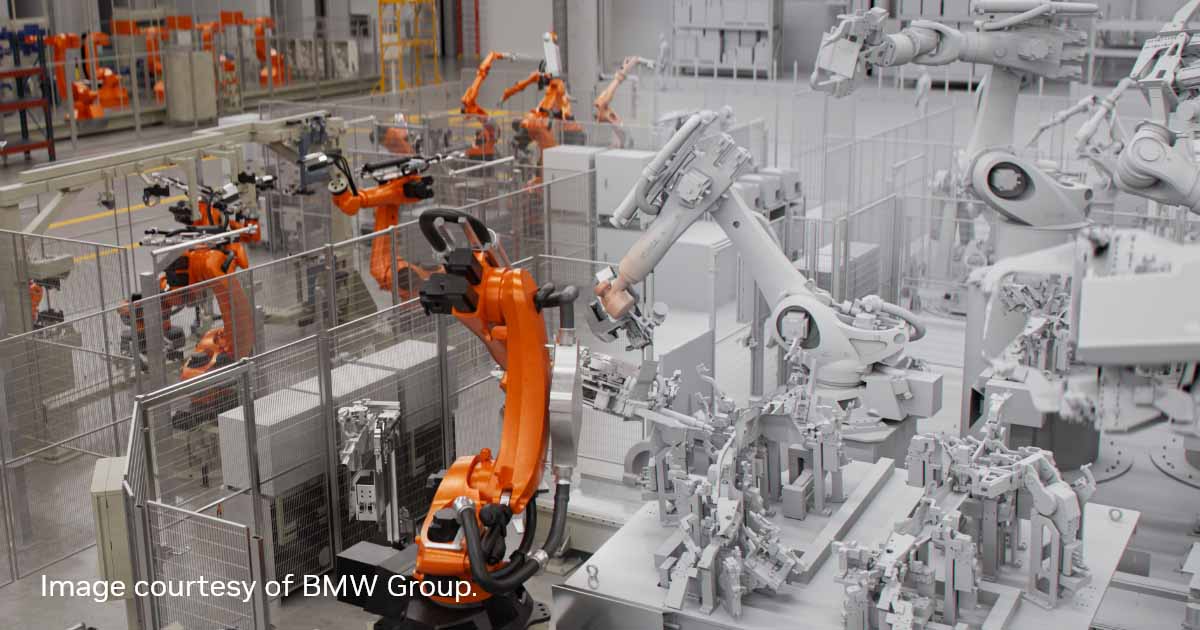
- Board Partners: Once the GPU chips are assembled and tested, they are sent to NVIDIA’s add-in board (AIB) partners (e.g., ASUS, MSI, Gigabyte, EVGA) for gaming graphics cards, or to server manufacturers for data center accelerators. These partners design and manufacture the Printed Circuit Boards (PCBs), integrate the GPU, memory, power delivery components, and cooling solutions to create the final product sold to consumers or businesses.
The Complex Journey: From Wafer to GPU
The transformation of an NVIDIA design into a functional GPU is a marvel of modern engineering, involving multiple highly specialized stages across different global entities.
Design and IP Creation
The journey begins at NVIDIA’s design centers worldwide. Here, engineers conceive and refine the architecture for new GPUs and AI processors. This involves:
- Conceptualization: Defining the overall architecture, instruction sets, and core functionalities of the chip (e.g., CUDA cores, Tensor Cores, RT Cores).
- Circuit Design: Translating the architecture into detailed electronic circuits, involving billions of transistors. This is done using highly sophisticated Electronic Design Automation (EDA) software.
- Verification and Simulation: Rigorously testing the design virtually to ensure it functions correctly, meets performance targets, and is free of errors before committing it to silicon. This stage is extremely resource-intensive and critical for avoiding costly re-spins.
- Physical Layout: Creating the precise layout of all components on the chip, adhering to the stringent rules of the chosen process node (e.g., 3nm, 5nm). The output is the GDSII file mentioned earlier.
Wafer Fabrication (The Foundry Step)
Once the design is finalized, the GDSII file is sent to the chosen foundry (e.g., TSMC). This is where the actual “manufacturing” of the silicon begins:
- Mask Creation: The GDSII data is used to create a series of “photomasks,” which are like stencils for each layer of the chip.
- Wafer Preparation: Silicon wafers (thin slices of extremely pure silicon) are prepared and cleaned.
- Photolithography: Layers of photosensitive material are applied to the wafer. The masks are then used to expose patterns onto these layers using ultraviolet light. This process is akin to developing a photograph, transferring the circuit design onto the wafer.
- Etching and Deposition: Exposed material is etched away, and new materials (conductors, insulators, semiconductors) are deposited onto the wafer. This cyclical process is repeated dozens, sometimes hundreds, of times, building up the complex 3D structure of transistors and interconnects.
- Doping: Impurities are intentionally introduced into specific areas of the silicon to alter its electrical properties, creating N-type and P-type semiconductors necessary for transistors.
- Testing at Wafer Level: Before cutting, the entire wafer undergoes initial electrical tests to identify defective dies, improving efficiency down the line.
Assembly, Testing, and Packaging (ATP)
After fabrication, the wafers are shipped from the foundry to OSAT companies for the next crucial stages:
- Wafer Dicing: The large silicon wafer, containing hundreds or thousands of individual chip “dies,” is precisely cut into separate dies.
- Die Bonding: Each good die is then mounted onto a lead frame or a substrate (a small circuit board that provides electrical connections and mechanical support).
- Wire Bonding/Flip-Chip: Tiny gold wires are bonded from the die to the substrate, or the die is “flipped” and bonded directly to the substrate using solder bumps (flip-chip technology), providing electrical connections.
- Encapsulation: The die and wires are encased in a protective plastic or ceramic material to shield them from environmental damage.
- Final Testing: The packaged chips undergo extensive functional and electrical testing to ensure they meet performance specifications and are free of defects. This can involve running diagnostic programs and checking for thermal stability.
Board Manufacturing and Final Product Assembly
The fully packaged and tested GPU chips (along with memory chips) are then shipped to NVIDIA’s board partners for final product integration:
- PCB Design and Manufacturing: Partners design and manufacture the Printed Circuit Boards (PCBs) that will house the GPU. These PCBs provide the necessary electrical pathways, power delivery, and connectivity.
- Component Assembly: The GPU chip, VRAM modules, power delivery components (VRMs), connectors, and other integrated circuits are mounted onto the PCB using automated surface-mount technology (SMT) processes.
- Cooling System Integration: Advanced cooling solutions (heatsinks, fans, liquid coolers) are attached to manage the significant heat generated by high-performance GPUs.
- Final System Integration: For data center accelerators, these boards are then integrated into larger server systems. For consumer graphics cards, they are packaged for sale.
Strategic Implications and Future Outlook
NVIDIA’s fabless model and global manufacturing ecosystem have profound strategic implications, shaping not only its own future but also the broader tech landscape.
Geopolitical Factors and Supply Chain Resilience
The highly concentrated nature of advanced semiconductor manufacturing (primarily in Taiwan with TSMC) has elevated it to a geopolitical flashpoint.
- US-China Tensions: The ongoing technological rivalry between the US and China, particularly concerning advanced chips, directly impacts NVIDIA. Export controls and trade restrictions can influence where NVIDIA’s chips are made and sold, necessitating careful strategic navigation.
- Taiwan’s Role: Taiwan’s critical role in chip production makes the stability of the region a global economic concern. Any disruption to TSMC’s operations would have catastrophic consequences for the tech industry, including NVIDIA.
- Push for Diversification and Reshoring: Governments worldwide, notably the US (via the CHIPS Act) and Europe, are actively pushing for domestic semiconductor manufacturing capacity to enhance supply chain resilience and reduce reliance on overseas fabs. While NVIDIA will likely continue to use TSMC, future strategies may involve leveraging new fabs in the US or Europe if they reach competitive process nodes and cost structures.
Innovation and Performance Leadership
The fabless model enables NVIDIA to maintain its innovation leadership:
- Focus on Differentiation: By outsourcing manufacturing, NVIDIA can dedicate its formidable engineering talent to architecting the next generation of GPUs and AI accelerators, focusing on breakthroughs in performance, efficiency, and new applications.
- Faster Iteration: Access to the latest foundry technologies allows NVIDIA to rapidly iterate on its designs, bringing new products to market with improved capabilities more quickly than if it had to build and equip its own fabs.
- Software Ecosystem: This hardware prowess is complemented by NVIDIA’s robust software ecosystem (CUDA, AI frameworks), which creates a powerful synergy and ecosystem lock-in, making its products indispensable for developers and researchers.

The Future of Semiconductor Manufacturing
The industry is constantly evolving, and NVIDIA will adapt to these changes:
- Advanced Packaging: As scaling transistors become more challenging, advanced packaging technologies (e.g., chiplets, 3D stacking) are becoming crucial. This allows different components (CPU cores, GPU cores, memory) to be integrated more tightly and efficiently within a single package, unlocking new levels of performance and modularity. NVIDIA is already a leader in this with its Hopper and Blackwell architectures.
- Chiplet Architectures: Moving away from monolithic dies to smaller, specialized “chiplets” that can be combined on an interposer offers greater flexibility, higher yields, and better performance-per-watt. NVIDIA is at the forefront of this trend.
- Continued Process Node Race: While the pace might slow, the race for smaller, more power-efficient process nodes (e.g., sub-3nm) will continue, driven by the insatiable demand for more computing power for AI and complex simulations. NVIDIA’s strong relationships with leading foundries will ensure it remains a beneficiary of these advancements.
In conclusion, “where NVIDIA manufactures” is not a single location but a complex, globally distributed network of highly specialized partners, primarily semiconductor foundries like TSMC and Samsung, complemented by a vast ecosystem of assembly, test, and board manufacturing companies. NVIDIA’s strategic brilliance lies in its focus on design and innovation, leveraging the world’s most advanced manufacturing capabilities without the burden of ownership. This fabless model is not just a business choice; it is a fundamental pillar of its success, allowing it to remain at the vanguard of technological progress in an increasingly interconnected and specialized world. As the tech landscape continues to evolve, NVIDIA’s ability to navigate geopolitical complexities, foster strategic partnerships, and continuously innovate within this global supply chain will dictate its ongoing leadership in the AI and computing revolution.
aViewFromTheCave is a participant in the Amazon Services LLC Associates Program, an affiliate advertising program designed to provide a means for sites to earn advertising fees by advertising and linking to Amazon.com. Amazon, the Amazon logo, AmazonSupply, and the AmazonSupply logo are trademarks of Amazon.com, Inc. or its affiliates. As an Amazon Associate we earn affiliate commissions from qualifying purchases.