
In the intricate world of semiconductor manufacturing, the question “Where does AMD make their chips?” doesn’t have a single, straightforward answer. Unlike the popular image of a company producing everything under one roof, Advanced Micro Devices (AMD) operates on a “fabless” model, a sophisticated strategy that has become increasingly common for leading chip designers. This means AMD designs its groundbreaking processors and graphics cards, but it entrusts the actual physical fabrication of these complex silicon marvels to highly specialized third-party manufacturing partners, primarily the world’s most advanced foundries. Understanding AMD’s manufacturing strategy requires delving into a global, multi-layered supply chain that exemplifies modern high-tech production.
The Fabless Model: AMD’s Strategic Approach
The semiconductor industry is characterized by incredibly high capital expenditure, rapid technological advancement, and a requirement for specialized expertise at every stage. For companies like AMD, maintaining their own cutting-edge fabrication plants (fabs) is no longer a sustainable or competitive strategy, leading to the widespread adoption of the fabless model.
Understanding the Fabless Semiconductor Company
A “fabless” semiconductor company, as the name suggests, lacks its own fabrication facilities. Instead, it focuses exclusively on the design, development, and marketing of integrated circuits, outsourcing the capital-intensive manufacturing processes to dedicated foundries. This division of labor allows companies like AMD to channel their resources into innovation – researching new architectures, optimizing performance, and developing intellectual property – rather than tying up billions of dollars in building and maintaining state-of-the-art manufacturing plants.
The advantages of this model are significant:
-
Lower Capital Expenditure: Fabs cost tens of billions of dollars to build and equip, with continuous investment required for upgrades. By outsourcing, AMD avoids this colossal financial burden.
-
Focus on Core Competencies: AMD can concentrate its talent and efforts on chip design, microarchitecture, software optimization, and market strategy, where its competitive edge truly lies.
-
Access to Cutting-Edge Technology: Foundries like TSMC are at the forefront of process technology. The fabless model allows AMD immediate access to the latest manufacturing nodes (e.g., 7nm, 5nm, 3nm) without having to develop them internally, ensuring their products remain competitive in terms of power efficiency and transistor density.
-
Flexibility and Scalability: Foundries can scale production up or down based on demand, providing AMD with greater agility in response to market fluctuations.
However, the fabless model also comes with its own set of challenges. Reliance on third-party manufacturers means less direct control over the entire production process, potential for supply chain bottlenecks, and increased competition for limited foundry capacity, especially during periods of high demand.
A Historical Perspective: From Integrated Device Manufacturer (IDM) to Fabless
AMD wasn’t always a fabless company. For many years, it operated as an Integrated Device Manufacturer (IDM), designing and manufacturing its own chips. This changed dramatically in 2009 when AMD spun off its manufacturing operations into a new entity called GlobalFoundries. This strategic divestiture was a pivotal moment, born out of the immense financial pressures of maintaining competitive fabs and the increasing costs of developing next-generation process technologies.
The move allowed AMD to shed the massive financial drain of fabrication, which had previously hampered its ability to invest sufficiently in research and development. This transition ultimately freed AMD to become a leaner, more agile, and design-focused company, a transformation that has been instrumental in its resurgence and competitive success against rivals like Intel. Today, GlobalFoundries continues to be an important foundry partner for certain AMD products, particularly chipsets and specialized components, though not typically for their most advanced CPUs and GPUs.
The Titans of Fabrication: AMD’s Key Manufacturing Partners
When AMD designs a new chip, they work closely with a select group of world-class semiconductor foundries to bring their designs to life. These foundries are the silent giants of the tech world, investing colossal sums in facilities and R&D to push the boundaries of silicon manufacturing.
TSMC: The Undisputed Leader in Advanced Chip Manufacturing
Taiwan Semiconductor Manufacturing Company (TSMC) stands as AMD’s most critical manufacturing partner for its leading-edge products. TSMC is the world’s largest dedicated independent semiconductor foundry, renowned for its technological prowess and ability to produce chips at the most advanced process nodes. Almost all of AMD’s cutting-edge CPUs (Ryzen for consumers, EPYC for data centers) and GPUs (Radeon for gaming, Instinct for AI/HPC) are fabricated by TSMC.
AMD leverages TSMC’s expertise for several key reasons:
-
Process Node Leadership: TSMC has consistently been at the forefront of process technology, often being the first to mass-produce chips on nodes like 7nm, 5nm, and now moving towards 3nm. These smaller nodes allow for more transistors on a given die size, leading to higher performance, greater power efficiency, and lower manufacturing costs per transistor.
-
Capacity and Reliability: TSMC operates numerous giga-fabs across Taiwan, with expansion plans in other regions, offering substantial manufacturing capacity and a reputation for high yield rates and consistent quality.
-
Advanced Packaging Technologies: Beyond just wafer fabrication, TSMC also offers advanced packaging solutions crucial for AMD’s chiplet designs (e.g., 3D V-Cache, 2.5D stacking for MI300). These technologies allow AMD to integrate multiple smaller chips (chiplets) into a single package, optimizing performance and cost.
TSMC’s primary fabrication facilities are located in Taiwan, a global hub for semiconductor manufacturing. However, in response to geopolitical pressures and supply chain diversification efforts, TSMC is also expanding its operations into other regions, including Arizona in the United States and Kumamoto, Japan, which could potentially serve AMD’s future needs from more geographically diverse locations.
Other Foundries and Specialized Production
While TSMC handles the bulk of AMD’s most advanced chip production, the company does utilize other foundries for specific products or components, often for reasons of cost-effectiveness, specialized process nodes, or diversification.
-
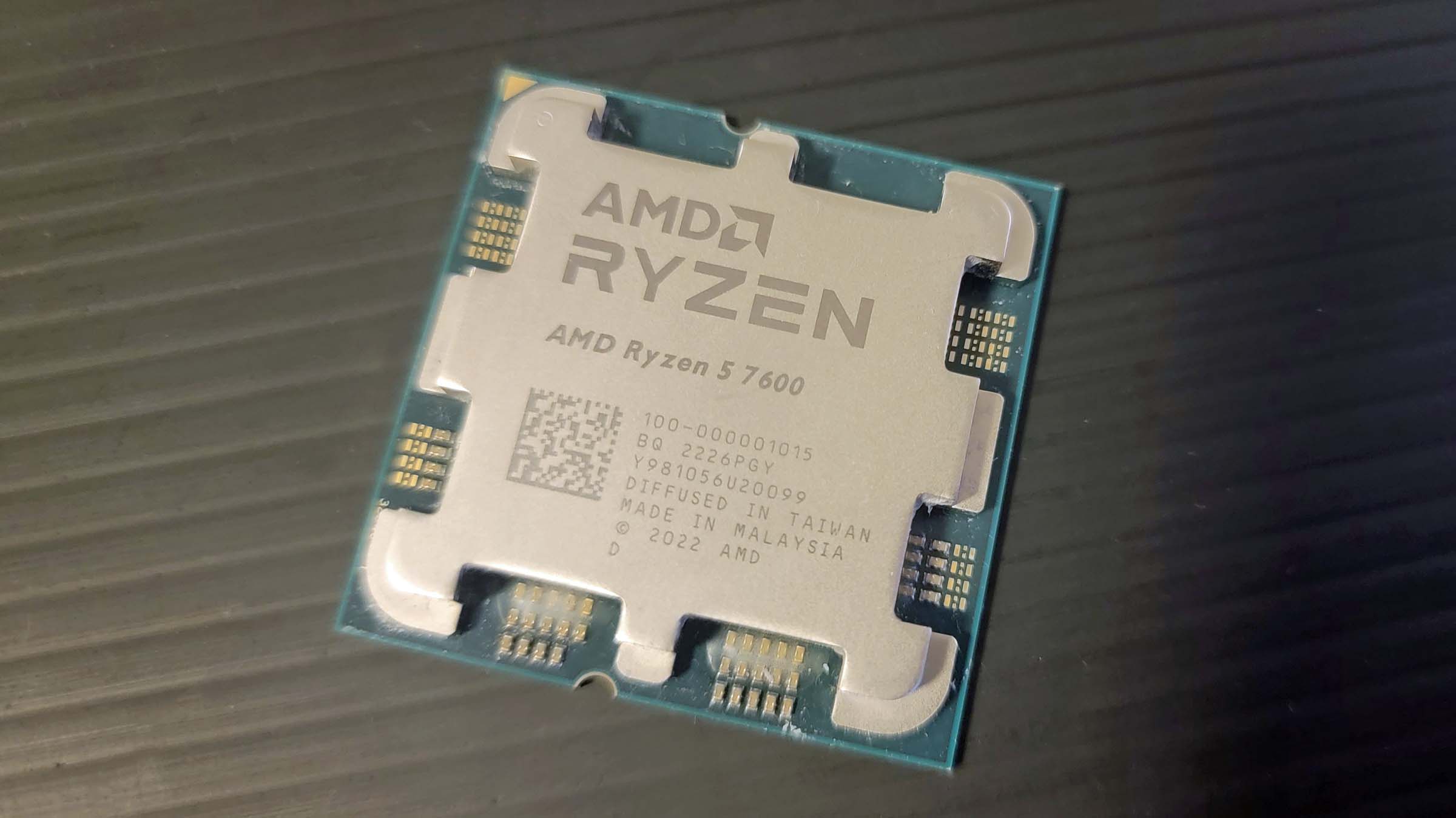
GlobalFoundries: As mentioned, GlobalFoundries, the spin-off of AMD’s former manufacturing arm, still plays a role. They often fabricate chipsets (the supporting chips on a motherboard), I/O dies (the parts of AMD’s chiplet designs that handle external communication), and potentially some older or less demanding product lines. GlobalFoundries has fabs in the United States (New York), Germany (Dresden), and Singapore.
-
Samsung Foundry: While Samsung Foundry is a major competitor to TSMC and manufactures chips for various companies, their partnership with AMD for core CPUs/GPUs has been less prominent compared to TSMC. However, the semiconductor landscape is dynamic, and foundry relationships can evolve. Samsung Foundry has facilities in South Korea and Texas, USA.
The choice of foundry depends on various factors including the required process node, cost, capacity, lead times, and the specific technological capabilities needed for a given chip design. For instance, less demanding components might be manufactured on older, more mature process nodes at a lower cost, which might not necessitate TSMC’s bleeding-edge capabilities.
Beyond the Foundry: The Global Semiconductor Supply Chain
The journey of an AMD chip doesn’t end when it leaves the foundry. The fabrication of the silicon wafer is just one, albeit crucial, step in a complex global supply chain that transforms raw silicon into a fully functional processor or graphics card.
Packaging, Assembly, and Testing (OSAT)
Once a foundry manufactures silicon wafers (thin circular slices of semiconductor material containing hundreds or thousands of individual chips, or “dies”), these wafers are then shipped to specialized Outsourced Semiconductor Assembly and Test (OSAT) companies. These companies perform critical post-fabrication steps:
-
Wafer Dicing: The individual dies are cut from the wafer.
-
Packaging: Each die is enclosed in a protective package (e.g., a ceramic or organic substrate) that provides electrical connections to the outside world and dissipates heat. This is where technologies like AMD’s chiplet designs and 3D V-Cache are integrated, involving sophisticated stacking and interconnections.
-
Assembly: Various components are assembled onto the package.
-
Testing: Rigorous electrical and functional tests are performed at various temperatures to ensure each chip meets specifications and is free of defects.
Key players in the OSAT segment include ASE Technology Holding (Taiwan), Amkor Technology (USA, with operations in Asia), and Siliconware Precision Industries Co., Ltd. (SPIL, Taiwan). These companies operate large-scale facilities predominantly in Asia, particularly Taiwan, China, Malaysia, and South Korea, which have developed specialized expertise and infrastructure for these labor-intensive and precision-critical processes.
Raw Materials and Equipment Providers
The entire semiconductor ecosystem relies on an even deeper layer of specialized companies providing the foundational elements:
-
Raw Materials: Companies like Shin-Etsu Chemical and SUMCO (Japan) are global leaders in producing ultra-pure silicon wafers, the fundamental building block of all chips. Other companies supply specialized gases, chemicals, and photoresists.
-
Manufacturing Equipment: The machinery used in modern fabs is incredibly complex and expensive. Dutch company ASML dominates the market for advanced photolithography equipment, which uses light to print circuit patterns onto silicon wafers. Other companies like Applied Materials, Lam Research, and KLA provide equipment for deposition, etching, and inspection.
This global network of suppliers highlights the extreme interdependence of the semiconductor industry. A disruption at any point in this chain – be it a natural disaster, geopolitical event, or even a factory fire – can have ripple effects across the entire technology world, impacting companies like AMD.
Strategic Implications and Future Outlook
AMD’s chosen manufacturing strategy has profound implications for its business, the broader tech industry, and even global geopolitics. The reliance on a few key partners, while strategically sound for innovation, also presents unique challenges.
Supply Chain Resilience and Geopolitical Considerations
The concentration of advanced semiconductor manufacturing in specific regions, most notably Taiwan, has become a significant geopolitical concern. The vast majority of the world’s most advanced chips, including those powering AMD’s latest products, originate from TSMC’s fabs in Taiwan. This geographical concentration creates a single point of failure in the event of natural disasters, power outages, or geopolitical instability in the region.
The COVID-19 pandemic vividly demonstrated the fragility of global supply chains, leading to widespread chip shortages that impacted industries from automotive to consumer electronics. In response, governments worldwide, including the United States with its CHIPS Act and the European Union with its European Chips Act, are investing billions to incentivize the domestic production of semiconductors and diversify the global manufacturing footprint. While this aims to build resilience, bringing leading-edge fabs online is a multi-year, multi-billion-dollar endeavor. AMD, while fabless, is deeply affected by these dynamics, as the availability and cost of manufacturing capacity directly impact its ability to deliver products to market.
Innovation and Performance
The fabless model enables AMD to maintain a laser focus on innovation in chip architecture and design. By offloading manufacturing complexities, AMD can dedicate its engineering talent and financial resources to pushing the boundaries of performance per watt, developing revolutionary chiplet designs, and integrating new features like AI accelerators. Its close partnership with TSMC ensures that these cutting-edge designs can be translated into silicon using the most advanced and efficient process technologies available.
The future of chip manufacturing for AMD will likely involve continued reliance on TSMC for leading-edge nodes, potentially diversifying some production to TSMC’s new fabs in the US and Japan. It will also involve an ongoing evolution of packaging technologies, as chiplets and 3D stacking become even more critical for delivering performance gains when traditional transistor scaling slows down. AMD’s ability to innovate in design and leverage the best manufacturing partners will continue to be critical for its competitive standing in the high-stakes semiconductor arena.
In conclusion, AMD does not “make” its chips in the traditional sense of owning the fabrication plants. Instead, it meticulously designs its chips and collaborates with a sophisticated network of global partners, predominantly TSMC, for fabrication. This fabless strategy has allowed AMD to thrive by focusing on its core strengths: innovation and design. The intricate global supply chain, spanning from raw materials to advanced packaging and testing, underscores the distributed and specialized nature of modern technology manufacturing, making the question of “where” a truly global and multi-faceted answer.
aViewFromTheCave is a participant in the Amazon Services LLC Associates Program, an affiliate advertising program designed to provide a means for sites to earn advertising fees by advertising and linking to Amazon.com. Amazon, the Amazon logo, AmazonSupply, and the AmazonSupply logo are trademarks of Amazon.com, Inc. or its affiliates. As an Amazon Associate we earn affiliate commissions from qualifying purchases.