
The digital heart of modern technology beats within semiconductor chips, and Advanced Micro Devices (AMD) stands as a pivotal player in their innovation and design. From powerful Ryzen CPUs and Radeon GPUs that drive gaming PCs and workstations to EPYC processors powering data centers and accelerators fueling AI research, AMD’s influence is pervasive. Yet, contrary to a common assumption, AMD does not own the massive, intricate fabrication plants – often called “fabs” or “foundries” – where these sophisticated silicon wonders are physically manufactured. Instead, AMD operates on a “fabless” model, a strategic choice that has profound implications for its business, the broader technology landscape, and the global semiconductor supply chain. Understanding “where AMD chips are made” requires a journey through a complex, interconnected web of design, manufacturing partnerships, and geopolitical considerations that span continents.

The Fabless Model: AMD’s Strategic Approach to Chip Production
AMD’s reliance on a fabless operational model is a cornerstone of its business strategy, enabling it to focus its resources on core competencies while leveraging the specialized expertise of global manufacturing giants. This approach has become increasingly prevalent among leading semiconductor firms due to the astronomical costs and technical complexities associated with building and operating state-of-the-art fabs.
Defining the Fabless Paradigm
The “fabless” model is characterized by semiconductor companies that design and market integrated circuits but outsource their fabrication (manufacturing) to third-party semiconductor foundries. This contrasts with “integrated device manufacturers” (IDMs) like Intel (though Intel is increasingly adopting elements of a hybrid model), which design, manufacture, and sell their own chips. For AMD, this means their engineers meticulously craft the architecture, circuit design, and intellectual property (IP) for their processors and graphics cards. Once the designs are finalized and verified, they are sent to manufacturing partners who then physically etch these designs onto silicon wafers using highly advanced lithography and deposition processes.
Advantages of Outsourcing Fabrication
The primary benefit of the fabless model is economic efficiency. Building and maintaining a leading-edge semiconductor fabrication plant can cost tens of billions of dollars and requires constant, massive investment in R&D and equipment upgrades to keep pace with Moore’s Law. By outsourcing, AMD avoids these prohibitive capital expenditures, freeing up capital to invest in research and development, talent acquisition, and market expansion. This allows AMD to concentrate on what it does best: innovation in chip architecture, microcode, and software optimization.
Furthermore, the fabless model offers flexibility. AMD can choose the foundry partner that offers the most advanced process technology suitable for its designs at any given time. This agility ensures access to cutting-edge manufacturing processes without the burden of owning and managing the fabs themselves, which would require significant lead times and massive internal shifts to upgrade production lines. It also mitigates the risk associated with underutilizing expensive fabs during market downturns or over-investing in a particular process technology that might quickly become obsolete.
Historical Context: From Integrated Device Manufacturer (IDM) to Fabless
Interestingly, AMD wasn’t always a fabless company. For many years, AMD operated as an IDM, owning and operating its own manufacturing facilities. However, the escalating costs and increasing complexity of semiconductor fabrication, coupled with intense competition, led AMD to spin off its manufacturing operations in 2009, creating GlobalFoundries. This strategic move allowed AMD to transition fully to a fabless model, a decision that many analysts now view as critical to its resurgence and competitive strength in the 2010s and beyond, enabling it to focus on design innovation rather than the daunting challenges of foundry operations.
The Core of Fabrication: Key Foundry Partners and Their Locations
The physical production of AMD chips, therefore, primarily takes place at the facilities of its chosen foundry partners. These partners are technological titans in their own right, operating some of the most sophisticated manufacturing sites on the planet.
TSMC: AMD’s Primary Manufacturing Giant
Taiwan Semiconductor Manufacturing Company (TSMC) is undoubtedly AMD’s most crucial manufacturing partner. Headquartered in Hsinchu, Taiwan, TSMC is the world’s largest dedicated independent semiconductor foundry. It is renowned for its state-of-the-art process technologies, consistently leading the industry in the development and mass production of the smallest and most power-efficient nodes, such as 7nm, 5nm, 4nm, and increasingly 3nm.
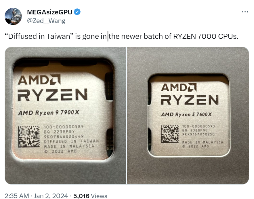
TSMC’s dominance in advanced nodes makes it the go-to choice for companies like AMD (and Apple, Qualcomm, Nvidia, amongst others) that require the absolute cutting edge in performance and power efficiency for their high-performance computing (HPC) products. The vast majority of AMD’s modern CPUs (Ryzen, EPYC) and GPUs (Radeon RX, Instinct) are fabricated at TSMC’s advanced facilities. These facilities are concentrated primarily in Taiwan, particularly in regions like Hsinchu, Taichung, and Tainan, which have evolved into global hubs for advanced semiconductor manufacturing. TSMC also has some manufacturing operations and offices in China, the United States, and Japan, though its most advanced production remains in Taiwan.
Geographic Strongholds of Advanced Semiconductor Manufacturing
The concentration of advanced semiconductor manufacturing in specific geographic locations, particularly Taiwan, South Korea (with Samsung Foundry being another major player), and increasingly, the United States and Europe, reflects decades of strategic investment, specialized expertise, and the development of robust supply chain ecosystems. These regions boast a unique combination of highly skilled engineering talent, access to necessary raw materials, a network of specialized equipment suppliers (like ASML for lithography), and government support.
Taiwan’s position as a global leader, exemplified by TSMC, is not just about the fabs themselves but the entire surrounding ecosystem. This includes companies specializing in packaging, testing, materials, and equipment, all within close proximity, creating an efficient and interdependent industrial cluster that is difficult to replicate elsewhere.
Other Partners and Specialized Production
While TSMC handles the bulk of AMD’s leading-edge CPU and GPU production, AMD utilizes other partners for specific components or older process technologies. GlobalFoundries, the company spun off from AMD’s original manufacturing arm, still plays a role. For example, some of the I/O (input/output) dies in AMD’s chiplet designs (which integrate multiple smaller “chiplets” or dies onto a single package) might be manufactured by GlobalFoundries on slightly older, more cost-effective nodes, allowing AMD to optimize for both performance and manufacturing cost. These I/O dies handle functions like PCIe, DDR memory controllers, and other interconnects, which don’t necessarily require the bleeding-edge performance of the core compute dies. GlobalFoundries has fabs in the United States (New York), Germany, and Singapore, offering AMD some geographical diversification for certain components.
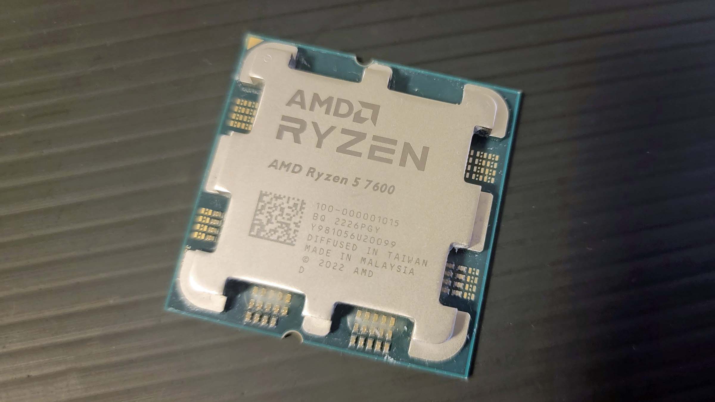
This multi-foundry strategy allows AMD to mitigate risks associated with relying on a single supplier and to strategically allocate different components to the most suitable and cost-effective manufacturing process.
Beyond the Wafer: The Intricate Stages of Semiconductor Manufacturing
The journey of an AMD chip doesn’t end once the silicon wafer emerges from the foundry. The manufacturing process is a multi-stage marathon that involves several distinct steps, each critical to delivering a functional, high-performance product.
Design and Architecture: The Genesis of an AMD Chip
Before any silicon is etched, an AMD chip begins as an intricate design within specialized software. This stage involves thousands of engineers at AMD’s design centers across the globe (including the U.S., Canada, India, etc.) meticulously crafting the core intellectual property, microarchitecture, and logic gates that define the chip’s functionality. This includes everything from the CPU cores and GPU shaders to memory controllers, I/O interfaces, and security features. Sophisticated simulation and verification tools are used to ensure the design is sound, performs as expected, and can be reliably manufactured. This “design house” aspect is AMD’s core strength and primary focus under the fabless model.
Packaging and Assembly: Connecting the Die to the World
Once the wafer is fabricated by a foundry like TSMC, it contains hundreds or thousands of individual chip “dies.” These dies must then be cut, tested, and “packaged.” The packaging stage is critical as it protects the delicate silicon die, provides electrical connections between the die and the circuit board, and helps dissipate heat. Modern chip packaging is incredibly complex, especially for AMD’s chiplet designs (e.g., in Ryzen and EPYC CPUs), which involve integrating multiple small dies onto a single substrate.
Advanced packaging techniques, such as 2.5D and 3D stacking, are increasingly employed to improve performance, power efficiency, and inter-chiplet communication. These packaging operations are often performed by specialized outsourced semiconductor assembly and test (OSAT) companies, which can be located in various countries, including Taiwan, China, Malaysia, and others with expertise in precision assembly.
Testing and Quality Assurance: Ensuring Performance and Reliability
After packaging, each individual chip undergoes rigorous testing. This involves functional testing to ensure all parts of the chip operate correctly, stress testing to check performance under various loads, and burn-in testing to weed out early failures. Advanced automated test equipment (ATE) is used to subject each chip to thousands of tests, verifying its adherence to design specifications and quality standards. Any faulty chips are discarded. This quality assurance process is paramount to AMD’s reputation and is carried out both by OSAT partners and often in AMD’s own facilities or by its designated contractors globally. Only chips that pass all tests are then prepared for shipment to customers or distributors.
Geopolitical Currents and Supply Chain Resilience
The global semiconductor supply chain is not immune to geopolitical forces, and the intricate network that manufactures AMD chips is increasingly being shaped by national interests, trade policies, and a push for greater resilience.
The Impact of Global Politics on Semiconductor Sourcing
The concentration of advanced chip manufacturing in specific regions, particularly Taiwan, has raised concerns among governments worldwide about supply chain vulnerabilities. Events such as the COVID-19 pandemic, which exposed fragilities in global logistics, and rising geopolitical tensions, particularly between the U.S. and China, have underscored the strategic importance of semiconductors. Governments now view access to advanced chips as a matter of national security and economic competitiveness.
Trade restrictions, export controls, and debates over technology transfer directly impact how and where chips are designed, manufactured, and sold. Companies like AMD must navigate a complex regulatory landscape, ensuring compliance while striving for an efficient and diversified supply chain. The potential for disruption, whether from natural disasters, political instability, or cyberattacks, necessitates constant vigilance and strategic planning.
Diversification Strategies and Regionalization Efforts
In response to these challenges, there’s a growing global effort to diversify semiconductor manufacturing and establish regional self-sufficiency. Nations are investing heavily in domestic chip production capabilities through initiatives like the U.S. CHIPS and Science Act and similar programs in Europe and Japan. The goal is to reduce reliance on a single region or country for advanced chip supply, thereby enhancing supply chain resilience.
While the fundamental economic advantages of specialized foundries in established hubs remain, the geopolitical imperative is driving investments in new fabs in places like Arizona (TSMC, Intel), Ohio (Intel), and Germany (Intel, TSMC exploring). For AMD, this means their future chip fabrication might become slightly more geographically distributed, though Taiwan is expected to remain the epicenter of leading-edge production for the foreseeable future due to its entrenched ecosystem and expertise.
Future of Semiconductor Manufacturing: Innovation and Self-Sufficiency
The future of where AMD chips are made will likely involve a continuous evolution of its fabless model, adapting to technological advancements and geopolitical realities. Innovation in materials science, lithography techniques (e.g., High-NA EUV), and advanced packaging will drive the next generation of performance and efficiency. At the same time, the push for regionalization will see new fabs emerge outside traditional strongholds.
AMD, as a leading designer, will continue to play a crucial role in pushing the boundaries of what’s possible with silicon, collaborating closely with its foundry partners to translate groundbreaking designs into tangible products. The journey from concept to silicon is a testament to global cooperation, technological marvel, and strategic foresight, underscoring that “where AMD chips are made” is a story far more intricate than a simple factory address. It’s a narrative of a global industry working in concert to power the digital world.
aViewFromTheCave is a participant in the Amazon Services LLC Associates Program, an affiliate advertising program designed to provide a means for sites to earn advertising fees by advertising and linking to Amazon.com. Amazon, the Amazon logo, AmazonSupply, and the AmazonSupply logo are trademarks of Amazon.com, Inc. or its affiliates. As an Amazon Associate we earn affiliate commissions from qualifying purchases.