At first glance, the question “what temperature does tin melt?” might seem like a simple trivia query, a fact easily googled and quickly forgotten. However, beneath this seemingly straightforward inquiry lies a wealth of scientific understanding and engineering significance that underpins countless technological advancements. For engineers, material scientists, product designers, and anyone involved in the manufacturing of electronic devices or high-tech components, tin’s melting point is not just a number; it is a critical parameter that dictates design choices, manufacturing processes, and ultimately, the reliability and longevity of modern technology.
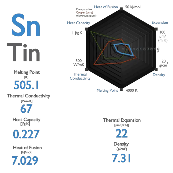
Tin, a soft, silvery-white metal, holds a unique position in the periodic table and in industrial applications. Its relatively low melting point, precisely 231.93 degrees Celsius (449.47 degrees Fahrenheit), makes it exceptionally versatile. This characteristic, coupled with its excellent electrical conductivity, corrosion resistance, and non-toxicity, has cemented its role in everything from the intricate circuits of a smartphone to the protective coatings of vital infrastructure. Understanding the nuances of this fundamental property is not merely academic; it is essential for innovating new materials, optimizing production techniques, and ensuring the robust performance of the tech we rely on daily. This article will delve into the scientific bedrock of tin’s melting point, explore its pervasive influence across various technological domains, and discuss the engineering challenges and future innovations driven by this unassuming yet indispensable element.
The Fundamental Science Behind Tin’s Melting Point
The melting point of any substance is a defining characteristic, a specific temperature at which it transitions from a solid to a liquid state. For tin, this precise threshold of 231.93°C is a consequence of its atomic structure and the forces that bind its atoms together. Delving into this fundamental science provides a clearer understanding of why tin behaves the way it does under thermal stress, a critical insight for its technological applications.
Defining Melting Point: A Critical Material Property
The melting point is a thermodynamic property representing the temperature at which the solid and liquid phases of a substance are in equilibrium at standard atmospheric pressure. At this specific temperature, the kinetic energy of the atoms or molecules within the solid becomes sufficient to overcome the intermolecular or interatomic forces holding them in a rigid lattice structure. For a crystalline solid like tin, this transition is typically sharp and well-defined. Below 231.93°C, tin maintains its solid, crystalline structure; above it, it transitions into a molten state. This critical point is not arbitrary; it’s a direct reflection of the material’s inherent properties and directly influences its processability and end-use performance in technological contexts. For instance, knowing tin’s melting point allows engineers to design precise heating profiles for soldering, ensuring components are joined effectively without overheating sensitive parts.
The Atomic Structure of Tin and its Influence
Tin (Sn) is a post-transition metal located in Group 14 of the periodic table, alongside carbon, silicon, and germanium. Its atomic structure, particularly its electron configuration and metallic bonding, plays a crucial role in determining its melting point. Tin typically forms a body-centered tetragonal crystal structure (known as β-tin or white tin) at room temperature. The atoms are arranged in a repeating pattern, held together by metallic bonds – a “sea” of delocalized electrons shared among a lattice of positive metal ions.
The strength of these metallic bonds directly correlates with the amount of energy required to break them and allow the atoms to move freely, i.e., to melt. Tin’s relatively low melting point compared to many other metals (like iron at 1538°C or copper at 1085°C) indicates that the metallic bonds in its crystalline lattice are not as strong. This is partly due to its atomic size and electron configuration, which result in weaker interatomic forces. This characteristic is precisely what makes tin so amenable to applications requiring easy melting and solidification, such as soldering, where a relatively low processing temperature is highly desirable to protect heat-sensitive electronic components.
Phase Transitions: Solid to Liquid
The process of melting is a first-order phase transition, meaning it involves a discontinuous change in entropy and volume. As heat energy is added to solid tin, its temperature rises until it reaches the melting point. At this point, the absorbed energy, known as the latent heat of fusion, is used to break the interatomic bonds and rearrange the atoms into a less ordered liquid state, rather than immediately increasing the temperature further. Only after all the solid tin has converted to liquid does the temperature of the molten tin begin to rise again with continued heat input.
This distinct phase transition with a specific latent heat is vital in many tech applications. In soldering, for example, the solder (often a tin alloy) absorbs heat at its melting point, becoming liquid and flowing into the joint. Upon cooling, it releases this latent heat as it solidifies, forming a strong metallurgical bond. Understanding this energy exchange is paramount for controlling soldering processes, preventing thermal shock to components, and ensuring the mechanical and electrical integrity of connections in electronic assemblies. The predictability of tin’s phase transition is a cornerstone of modern electronics manufacturing.
Tin in Modern Technology: Beyond Basic Metallurgy
Tin’s relatively low melting point, coupled with its other advantageous properties, has elevated it from a mere metal to an indispensable component in the vast landscape of modern technology. Its applications extend far beyond traditional metallurgy, permeating crucial sectors from microelectronics to advanced materials.
The Indispensable Role of Solder in Electronics
Perhaps the most prominent technological application of tin’s melting characteristics is its role in solder. Solder is an alloy that is melted to join electrical components together, forming both electrical connections and mechanical bonds. Historically, lead-tin solders were standard due to their excellent wetting properties and low melting points. However, with increasing environmental regulations and health concerns regarding lead, lead-free solders have become the industry norm. These lead-free alternatives primarily consist of tin, often alloyed with other elements like silver and copper (SAC alloys).
The melting point of pure tin (231.93°C) serves as the baseline for these alloys. While SAC alloys typically have slightly higher melting points (e.g., SAC305 melts around 217-220°C, a eutectic temperature lower than pure tin but higher than traditional lead-tin), tin remains the dominant component because it provides the foundational low melting point, excellent electrical conductivity, and good adhesion necessary for reliable interconnections. The precise control over the solder’s melting and reflow temperature is critical for surface-mount technology (SMT) and through-hole soldering processes, where delicate electronic components must withstand specific thermal profiles without damage. Without tin’s specific thermal behavior, the high-density, reliable circuit boards that power everything from smartphones to supercomputers would be impossible to manufacture efficiently.
Tin Plating: Corrosion Resistance and Conductivity
Beyond soldering, tin’s relatively low melting point contributes to its utility in electroplating and hot-dip coating processes. Tin plating involves coating a substrate (often copper, steel, or brass) with a thin layer of tin. This process leverages tin’s attributes to provide several critical benefits in tech:
- Corrosion Resistance: Tin forms a protective oxide layer that shields the underlying metal from environmental degradation, crucial for connectors, busbars, and components exposed to moisture or corrosive agents.
- Excellent Solderability: A tin-plated surface maintains its ability to be easily soldered, even after prolonged storage, ensuring reliable connections in future assembly processes.
- Electrical Conductivity: While not as conductive as copper or silver, tin plating provides good electrical continuity, which is vital for electrical contacts and terminals.
- Reduced Fretting Corrosion: In separable electrical connectors, tin plating helps minimize fretting corrosion, a common failure mode caused by small movements between mating surfaces.
The relatively low melting point means that tin can be applied through hot-dip processes at temperatures that do not excessively stress the base material, or through electroplating techniques which are also influenced by the material’s inherent thermal properties during subsequent reflow stages. This dual benefit of protection and connectivity makes tin plating an unsung hero in many electronic and automotive applications.
Emerging Applications: From Anodes to Quantum Computing
The versatility of tin extends to cutting-edge technological frontiers, with its melting point often playing an indirect yet fundamental role in its suitability.
- Lithium-Ion Batteries: Tin-based materials are being explored as anode materials for next-generation lithium-ion batteries. Tin can alloy with lithium, offering a much higher theoretical capacity than traditional graphite anodes. While the melting point of tin itself isn’t directly involved in battery operation, the ability to process tin into various nanostructures and thin films (often via techniques involving controlled heating and cooling) is crucial for optimizing its electrochemical performance.
- Perovskite Solar Cells: Tin is increasingly being used as a constituent in the active layers of perovskite solar cells, a rapidly developing photovoltaic technology. Here, tin often forms compounds (like tin iodide) that are processed at relatively low temperatures, making tin-based perovskites appealing for cost-effective manufacturing and flexible solar cell applications.
- Topological Insulators and Quantum Computing: In advanced physics and materials science, tin and its compounds are subjects of research for their potential in topological insulators – materials that behave as insulators in their bulk but conduct electricity along their surface. These materials hold promise for applications in quantum computing due to their unique electronic properties. The ability to synthesize tin-based crystals and thin films with precise structural control, often involving specific temperature profiles, is fundamental to exploring these quantum phenomena.
These diverse applications underscore that while the specific melting temperature of 231.93°C is a single data point, its implications ripple through a vast array of high-tech industries, enabling innovation and driving progress.
Engineering Challenges and Innovations Driven by Tin’s Properties
Tin’s unique thermal properties, especially its melting point, present both significant engineering challenges and fertile ground for innovation. As technology demands smaller, faster, and more reliable devices, the meticulous management of tin and its alloys becomes ever more critical.
Lead-Free Solders: A Regulatory and Technical Revolution
The shift from lead-tin to lead-free solders, driven by environmental regulations like RoHS (Restriction of Hazardous Substances) in the European Union, represents one of the most significant engineering revolutions influenced by tin’s properties. While beneficial for public health and the environment, this transition introduced substantial technical challenges:
- Higher Melting Points: Lead-free solders (predominantly tin-silver-copper alloys) generally have higher melting points (e.g., 217-220°C) compared to eutectic lead-tin solder (183°C). This necessitates higher processing temperatures during manufacturing, which can stress delicate electronic components and require adjustments to reflow ovens and soldering equipment.
- Wetting and Reliability: Achieving good “wetting” (how well molten solder spreads and adheres to a surface) with lead-free solders can be more challenging. Engineers have had to develop new flux chemistries and optimize thermal profiles to ensure reliable, void-free solder joints.
- Tin Whiskers: A unique metallurgical phenomenon associated with pure tin and high-tin alloys is the growth of “tin whiskers” – microscopic, hair-like crystalline structures that can grow from the surface of tin plating. These whiskers can cause electrical short circuits, particularly in tightly packed electronic assemblies. Mitigating whisker growth through alloying (e.g., with nickel or copper) and controlled plating processes is an ongoing engineering challenge crucial for product reliability.
Innovations in solder paste formulations, reflow oven technologies, and real-time process monitoring have been instrumental in overcoming these challenges, ensuring that lead-free electronics meet stringent reliability standards.
Thermal Management in Electronic Devices
As electronic devices become more powerful and miniaturized, managing heat dissipation is paramount. While tin-based solders connect components, they also play a role in thermal pathways. The specific thermal conductivity of tin and its alloys influences how efficiently heat is transferred away from critical components like CPUs and GPUs. Engineers meticulously design thermal interfaces, often using thermal greases or pads, but the inherent thermal properties of solder joints themselves contribute to the overall thermal management strategy.
Moreover, the melting point of solder directly impacts the device’s operational temperature limits. If a device operates in an extremely hot environment, there’s a risk of the solder joints softening or melting, leading to catastrophic failure. Therefore, engineers must select solder alloys with appropriate melting characteristics for high-temperature applications or design robust cooling systems to keep internal temperatures well below the solder’s melting threshold, ensuring device longevity and performance.
Advanced Manufacturing Techniques: Reflow Soldering and Wave Soldering
The precise thermal behavior of tin alloys is central to modern electronic assembly techniques.
- Reflow Soldering: This process, primarily used for surface-mount devices (SMD), involves applying solder paste (a mixture of solder powder and flux) to circuit board pads, placing components, and then passing the board through a reflow oven. The oven has precisely controlled temperature zones: preheat, soak, reflow (where the solder melts), and cooling. The exact melting point of the tin-based solder dictates the peak temperature and dwell time in the reflow zone. Engineering these thermal profiles is an intricate dance, aiming to fully melt the solder for robust joints without causing thermal damage to sensitive components or the PCB itself.
- Wave Soldering: Used mainly for through-hole components, this technique involves passing a PCB over a wave of molten solder. The temperature of this molten solder bath is critical; it must be maintained above the solder’s melting point to ensure proper wetting and formation of reliable joints. For lead-free solders, the wave temperature is significantly higher (e.g., 255-270°C) compared to leaded solder, requiring more robust PCB materials and component specifications.
Continuous innovation in these manufacturing processes, driven by a deep understanding of tin’s thermal properties, enables the mass production of high-quality, complex electronic systems that define our digital age.
Impact on Product Design and Longevity
The inherent properties of tin, particularly its melting point, are not just manufacturing considerations; they deeply influence the initial design and the long-term reliability of electronic products. Design choices are often a direct response to tin’s characteristics, aiming to optimize performance and durability.
Ensuring Reliability in Extreme Environments
Products designed for harsh environments – such as automotive electronics, aerospace systems, industrial controls, or military hardware – face extreme temperature fluctuations, vibrations, and corrosive conditions. In these scenarios, the melting point of tin-based solders becomes a critical design parameter. Engineers must select solder alloys with melting characteristics that are well above the maximum anticipated operating temperature, providing a sufficient safety margin. For example, higher-temperature solders might be employed in under-hood automotive applications where temperatures can exceed 150°C.
Furthermore, thermal cycling (repeated heating and cooling) can induce fatigue in solder joints. The mechanical properties of tin alloys, which are temperature-dependent, play a crucial role in predicting how long these joints will last. Design methodologies incorporate extensive testing and modeling to ensure that solder connections can withstand these stresses over the product’s intended lifespan. The transition to lead-free solders has complicated this aspect, as some lead-free alloys exhibit different fatigue characteristics compared to their leaded predecessors, necessitating updated design guidelines and qualification standards.
Miniaturization and Heat Dissipation Considerations
The relentless drive towards miniaturization in electronics poses significant challenges for thermal management and solder joint integrity. As components become smaller and packed more densely, the amount of heat generated per unit area increases dramatically. While tin’s low melting point facilitates easy processing, it also means that localized hot spots could potentially lead to solder reflow or degradation if not managed effectively.
Designers must consider the thermal conductivity of the entire assembly, including the PCB material, component packages, and especially the tin-based solder joints themselves. Innovative cooling solutions, such as heat sinks, thermal vias, and advanced substrate materials, are often necessary to keep the operating temperatures of critical components well below the solder’s melting point. Moreover, the mechanical strength of miniature solder joints is also crucial, and the microstructure of the tin alloy formed during solidification (influenced by cooling rates) is a key factor in preventing early mechanical failure. This interdependency between tin’s thermal properties, physical dimensions, and operational performance underscores its fundamental role in miniaturized electronics.
Recycling and Sustainability in the Tin Lifecycle
The properties of tin, including its relatively low melting point, also have significant implications for the sustainability and circular economy of electronic products. With the ever-increasing volume of e-waste, efficient recycling and material recovery are vital.
- Ease of Recycling: Tin’s low melting point makes it relatively energy-efficient to melt and refine compared to many other metals. This facilitates its recovery from end-of-life electronic products. Once components are disassembled, the tin-based solder can be melted down, separated, and reprocessed for reuse in new products.
- Lead-Free Advantage: The move to lead-free solders has simplified the recycling process by removing a hazardous contaminant. This allows for cleaner recycling streams and reduces the environmental impact of manufacturing new products from recycled materials.
- Resource Management: Tin is not an infinitely abundant resource. Understanding its properties and lifecycle is crucial for developing sustainable practices, from responsible mining to efficient recycling, ensuring a continuous supply for future technological innovations.
By considering tin’s full lifecycle, from its initial melting point facilitating manufacturing to its re-melting for recycling, the tech industry can work towards more environmentally responsible product design and resource management, leveraging the inherent characteristics of this versatile metal.
Future Perspectives: Pushing the Boundaries of Tin-Based Materials
The understanding of tin’s melting point and associated properties has been a cornerstone of technological advancement for decades. Yet, the journey of innovation with tin is far from over. Future research and development are pushing the boundaries, exploring new alloys, nanoscale structures, and advanced modeling to unlock even greater potential from this essential element.
Alloying for Tailored Properties
While pure tin has a distinct melting point, its true versatility shines through in alloys. The future will see continued innovation in creating new tin-based alloys with precisely tailored properties. This involves:
- Ultra-low Melting Point Solders: For highly heat-sensitive components or flexible electronics that cannot withstand high processing temperatures, research focuses on tin alloys (often with bismuth or indium) that melt at even lower temperatures. These eutectic or near-eutectic alloys aim to reduce thermal stress during assembly.
- High-Reliability, High-Temperature Solders: Conversely, for extreme environment applications, there’s a push to develop tin alloys that maintain mechanical integrity and electrical connectivity at higher operational temperatures, potentially involving additions of antimony, silver, or other elements that raise the softening point.
- Novel Intermetallic Compounds: Beyond traditional alloys, researchers are exploring complex intermetallic compounds involving tin that exhibit unique electronic, magnetic, or superconducting properties, opening doors for entirely new classes of materials for advanced computing and sensing.
The ability to finely tune the melting behavior and other properties through alloying will remain a critical pathway for addressing emerging challenges in electronics and materials science.
Nanotechnology and Tin’s Potential
The realm of nanotechnology offers exciting prospects for tin. When tin is engineered at the nanoscale, its properties can diverge significantly from its bulk form.
- Nanoscale Solder: Solder pastes containing tin nanoparticles can achieve lower reflow temperatures due to the “size effect,” where the melting point of a material decreases as particle size shrinks. This could enable ultra-low-temperature soldering for extremely delicate substrates.
- Tin Nanowires and Quantum Dots: Fabricating tin into nanowires or quantum dots can unlock novel electronic and optical properties. These nanostructures might find applications in quantum dots for displays, high-efficiency catalysts, or components in advanced sensors and thermoelectric devices. The synthesis of these nanostructures often involves precise temperature control and understanding the melting behavior at the atomic scale.
- Improved Battery Anodes: As mentioned earlier, tin nanoparticles and nanostructures are being intensely studied for next-generation battery anodes. Their high surface area and ability to better accommodate volume changes during lithium insertion and extraction could lead to higher capacity and longer-lasting batteries for portable devices and electric vehicles.

Predictive Modeling and Material Science
The future of tin-based materials development will heavily rely on advanced computational tools and predictive modeling. Techniques like Density Functional Theory (DFT) and CALPHAD (CALculation of PHAse Diagrams) allow material scientists to simulate the atomic interactions and phase transformations of tin and its alloys. This enables:
- Virtual Alloy Design: Before expensive and time-consuming experimental work, new alloy compositions can be virtually screened for desired properties, including melting point, mechanical strength, and electrical conductivity.
- Process Optimization: Simulations can model the heating and cooling profiles in manufacturing processes, helping engineers optimize parameters to achieve ideal solder joint microstructures or crystal growth.
- Failure Prediction: Understanding how thermal stresses and fatigue accumulate in tin-based materials under various conditions can lead to more accurate predictions of product lifespan and failure modes, further enhancing reliability.
By combining fundamental scientific understanding with cutting-edge computational power, the ability to precisely control and manipulate tin’s properties, including its critical melting point, will continue to drive innovation across the entire spectrum of technology, from the smallest microchip to the most powerful quantum computer. The seemingly simple question of “what temperature does tin melt?” thus opens a window into a complex and evolving technological landscape.
aViewFromTheCave is a participant in the Amazon Services LLC Associates Program, an affiliate advertising program designed to provide a means for sites to earn advertising fees by advertising and linking to Amazon.com. Amazon, the Amazon logo, AmazonSupply, and the AmazonSupply logo are trademarks of Amazon.com, Inc. or its affiliates. As an Amazon Associate we earn affiliate commissions from qualifying purchases.