
In the landscape of modern technology, we often focus on the macro-level achievements: the sleek finish of a smartphone, the speed of a neural network, or the range of an electric vehicle. However, the true frontiers of innovation are currently being contested at a scale that is invisible to the naked eye. At the heart of this microscopic revolution is a fundamental concept from chemistry and physics that has become a cornerstone of technological development: the ionic radius.
While traditionally relegated to introductory chemistry textbooks, the ionic radius has emerged as a critical metric for hardware engineers, battery scientists, and semiconductor architects. Understanding what the ionic radius is, how it is measured, and how it dictates the behavior of materials is essential for anyone looking to understand the next decade of technological evolution.

Defining the Ionic Radius in the Context of High-Performance Hardware
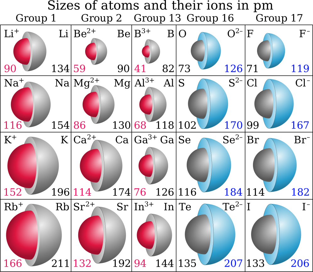
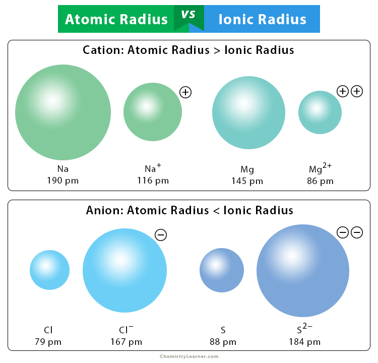
At its simplest level, the ionic radius is the measure of an atom’s ion in a crystal lattice. It is half the distance between two gas atoms that are just touching each other. When an atom loses or gains electrons to become an ion, its physical footprint changes. Cations (positively charged ions) shrink as they lose electron shells and experience increased nuclear pull, while anions (negatively charged ions) expand as the addition of electrons increases inter-electronic repulsion.
The Atomic Yardstick for Tech Engineering
In the world of technology, these measurements are not merely theoretical. They represent the “clearance” required for particles to move through solid structures. If we think of a semiconductor or a battery membrane as a high-tech sieve, the ionic radius determines which particles can pass through and how much energy is required to move them.
For instance, in the development of sophisticated hardware, engineers must account for how ions sit within a crystal structure. If an ion is too large, it can cause mechanical strain, leading to the eventual degradation of the component. If it is too small, it may not interact effectively with the surrounding electronic field. This precision is what allows for the creation of stable, long-lasting digital components.
Periodic Trends and Engineering Constraints
The predictability of the ionic radius across the periodic table allows tech researchers to swap materials to achieve specific results. As one moves down a group in the periodic table, the ionic radius increases due to the addition of electron shells. Conversely, as one moves across a period, the radius typically decreases.
Hardware designers use these trends to “tune” materials. For example, if a specific ceramic used in a sensor needs to be more sensitive to pressure, engineers might replace one ion with another of a slightly different radius to alter the internal tension of the material. This level of atomic-scale manipulation is what separates current-gen sensors from the high-precision tools required for autonomous driving and advanced robotics.
The Energy Frontier: How Ionic Radius Dictates the Future of Batteries
Perhaps the most visible application of the ionic radius in current technology trends is in the field of energy storage. The “Lithium-Ion” battery, which powers everything from iPhones to Tesla Model S vehicles, is named specifically after the ion it utilizes. The reason lithium was chosen as the industry standard is inextricably linked to its ionic radius.
Lithium vs. Sodium: A Size Comparison
Lithium has a remarkably small ionic radius (approximately 0.76 Å). This small size allows lithium ions to move quickly and easily into the interstitial spaces of an electrode, a process known as intercalation. This rapid movement is what allows for fast charging and high power density.
However, as the tech industry faces lithium shortages and rising costs, attention has shifted to Sodium-ion (Na-ion) batteries. Sodium is more abundant and cheaper, but it possesses a larger ionic radius (approximately 1.02 Å). This 25% increase in size presents a massive engineering hurdle. Because the sodium ion is larger, it moves more slowly through materials and can physically “stretch” the battery’s internal structure during charge cycles, leading to a shorter lifespan. The current software-driven research in battery tech is focused on designing new carbon-based anodes with larger “gates” to accommodate the larger radius of the sodium ion without sacrificing structural integrity.
Solid-State Electrolytes and the Volumetric Challenge
The tech industry is currently racing toward the “holy grail” of energy: the solid-state battery. Unlike traditional batteries that use liquid electrolytes, solid-state versions use solid ceramics or polymers. In this medium, the ionic radius is the primary factor in determining “ionic conductivity.”
If the radius of the moving ion is not perfectly matched to the “tunnels” within the solid electrolyte, the battery will be inefficient or prone to overheating. Tech companies like QuantumScape and Toyota are investing billions into atomic-level modeling to find the perfect lattice-to-radius ratio. This is not just chemistry; it is high-level mechanical engineering at a scale where the “parts” are individual atoms.
Semiconductor Fabrication and the Precision of Doping
The semiconductor industry is currently pushing the limits of Moore’s Law, moving from 5nm to 3nm and eventually 2nm processes. At these scales, the ionic radius becomes a limiting factor in how chips are manufactured and how they perform.
Lattice Mismatch and Strain Engineering
In semiconductor fabrication, “doping” is the process of adding impurities to a pure crystal of silicon to change its electrical properties. If a technician introduces an ion with a significantly different radius than the silicon atoms it is replacing, it creates “strain” in the crystal lattice.
While strain sounds negative, “strain engineering” is a sophisticated tech tutorial in itself. By carefully selecting ions with specific radii, engineers can stretch or compress the silicon atoms, which changes the path electrons take. This can actually speed up the movement of electrons, resulting in faster processors that consume less power. Without a precise understanding of the ionic radius, the high-performance chips found in modern AI servers would be impossible to manufacture.
The Pursuit of the 2-Nanometer Node
As we approach the 2nm node, the physical space within a transistor is so small that a single ion with a large radius could block the entire channel. We are reaching a point in digital security and hardware design where “atomic variability” is a risk factor. Software tools used in Electronic Design Automation (EDA) must now account for the specific ionic radii of every material used in the stack to prevent “leakage current,” where electrons jump across boundaries because the atomic packing isn’t tight enough.
AI-Driven Discovery: Digital Twins of the Atomic World
The most exciting crossover between software and the ionic radius lies in Artificial Intelligence and Machine Learning. Historically, discovering a new material with the right atomic properties took decades of trial and error in a physical lab. Today, AI tools are shortening this cycle to months.
Predictive Modeling and Deep Learning
Modern AI tools like Google’s GNoME (Graph Networks for Materials Exploration) have predicted the stability of millions of new crystals. These AI models use the ionic radius as a primary input feature. By training on the radii of known stable materials, the software can predict how a hypothetical material will behave.
For example, if an AI is tasked with finding a new superconductor, it will scan through combinations of elements, calculating how the different ionic radii will fit together. If the “geometric frustration” (a result of mismatched radii) is too high, the AI discards the candidate before a single cent is spent in a lab. This fusion of software and chemistry is the primary driver of the current “materials gold rush.”
Software Ecosystems for Material Informatics
There is a growing niche of “Material Informatics” software—platforms like Citrine Informatics or Matmatch—that allow companies to search for materials based on precise atomic specs. A hardware startup looking for a specific thermal expansion coefficient can filter materials by the ionic radii of their constituent parts. This digitization of the periodic table is a trend that is transforming the R&D departments of every major tech firm from Apple to Intel.
Future Implications for Quantum Computing and Nanotechnology
As we look toward the future of technology, the ionic radius will continue to be the gatekeeper of innovation, particularly in the realms of quantum computing and advanced nanotechnology.
Qubits and Ionic Control
In trapped-ion quantum computers, individual ions are held in place by electromagnetic fields to serve as qubits. The precision required to manipulate these ions is dependent on their mass and their charge-to-radius ratio. The “size” of the ion influences how it reacts to the lasers used to change its state. Engineering these systems requires a level of control over the ionic radius that was unthinkable twenty years ago.
The Miniaturization of Everything
From targeted drug delivery in med-tech to the creation of ultra-dense memory storage, the ability to predict and utilize the ionic radius is the difference between a theoretical concept and a market-ready product. As we move deeper into the age of nanotechnology, we are no longer just building with blocks; we are building with the specific, measured volumes of ions.
The ionic radius is more than just a measurement of an atom’s reach; it is the fundamental constraint of the physical world that defines the limits of our digital ambitions. Whether it is the speed of your next smartphone, the range of your electric car, or the security of a global server network, the invisible dimensions of the ionic radius are the silent architects of the modern technological era. Understanding this metric is not just for scientists—it is for anyone who wants to grasp the future of tech.
aViewFromTheCave is a participant in the Amazon Services LLC Associates Program, an affiliate advertising program designed to provide a means for sites to earn advertising fees by advertising and linking to Amazon.com. Amazon, the Amazon logo, AmazonSupply, and the AmazonSupply logo are trademarks of Amazon.com, Inc. or its affiliates. As an Amazon Associate we earn affiliate commissions from qualifying purchases.