Gold PVD, or Physical Vapor Deposition of gold, represents a sophisticated technological advancement in surface coating, offering a superior alternative to traditional gold plating methods. Far from a simple cosmetic treatment, PVD is a high-tech manufacturing process that deposits a thin, durable layer of actual gold onto a substrate material through an intricate vacuum-based technique. This process is prized across industries—from high-end consumer electronics and watches to critical medical devices and aerospace components—for its ability to imbue materials with enhanced properties, including exceptional hardness, scratch resistance, and an aesthetically consistent finish that significantly outlasts conventional coatings. Understanding Gold PVD requires delving into the precise physics and engineering that govern its application, positioning it firmly within the realm of advanced material science and industrial technology.

The Technology Behind PVD Coatings
Physical Vapor Deposition is a blanket term for a family of vacuum deposition methods used to produce thin films and coatings. At its core, PVD involves creating a vaporized form of a source material (in this case, gold) and then allowing that vapor to condense as a thin, solid film on the surface of an object, known as the substrate. This process occurs in a highly controlled vacuum environment, differentiating it sharply from electroplating or chemical deposition techniques. The technological brilliance of PVD lies in its ability to generate coatings with properties far superior to those achieved by traditional methods, thanks to the atomic-level control over film formation.
Physical Vapor Deposition Explained
The fundamental principle of PVD relies on a series of physical processes: evaporation or sputtering of a source material, transport of the vaporized atoms or molecules through a vacuum or low-pressure gaseous environment, and finally, their condensation and nucleation on the substrate surface. Unlike chemical reactions, PVD is a purely physical process, minimizing unwanted contaminants and allowing for exceptionally pure, dense, and well-adhered films. During the deposition, energy is imparted to the gold atoms, often through plasma generation, causing them to bond strongly with the substrate at a molecular level. This robust metallurgical bond is a cornerstone of PVD’s durability, providing an integral coating rather than a superficial layer.
Advantages Over Traditional Coating Methods
The technological evolution to PVD was driven by inherent limitations in older coating technologies. Electroplating, for instance, often results in a porous coating with relatively weak adhesion and inconsistent thickness, and typically involves toxic chemicals. PVD, conversely, yields a dense, non-porous film with superior adhesion, often exceeding the bond strength of the substrate material itself. The process operates without toxic chemicals, reducing environmental impact and improving worker safety, aligning with modern green manufacturing initiatives. Furthermore, PVD allows for precise control over film thickness, composition, and even microstructure, enabling the engineering of coatings with specific mechanical, optical, or electrical properties. This level of control is virtually unattainable with conventional liquid-based deposition techniques.
The Gold PVD Process: An In-Depth Look
Executing a successful Gold PVD coating requires a meticulously controlled, multi-stage technological process. Each step, from initial cleaning to the final deposition, is critical to achieving the high-performance and aesthetic qualities synonymous with PVD.
Substrate Preparation
The integrity of any PVD coating is fundamentally dependent on the cleanliness and surface condition of the substrate. This initial phase is rigorously scientific, involving multiple cleaning steps designed to remove all traces of contaminants such as oils, greases, dust, and oxides. Common techniques include ultrasonic cleaning, solvent degreasing, and plasma cleaning, often followed by an ion bombardment within the vacuum chamber itself. This atomic-scale etching further prepares the surface, enhancing “active” sites for the gold atoms to bond with, ensuring maximum adhesion and preventing defects in the final film. Skipping or compromising this stage inevitably leads to poor coating adhesion, flaking, or inconsistent finish.
The Vacuum Chamber and Target Material
The heart of the PVD process is the vacuum chamber, a sophisticated piece of engineering designed to maintain an ultra-low pressure environment. This vacuum is essential to prevent contamination from ambient gases and to ensure that the vaporized gold atoms travel directly to the substrate without collision or reaction with other molecules. Inside, a pure solid gold “target” is positioned. This target serves as the source material for the coating. The chamber also contains fixtures to hold and often rotate the items (substrates) to be coated, ensuring uniform film thickness across all surfaces. Advanced vacuum pumps and gauges constantly monitor and control the pressure, which is critical for the consistency and quality of the deposited layer.
Vaporization and Ionization
Within the vacuum chamber, the gold target is subjected to high-energy bombardment, causing its atoms to vaporize and, in many cases, ionize. Two primary methods are employed for this:
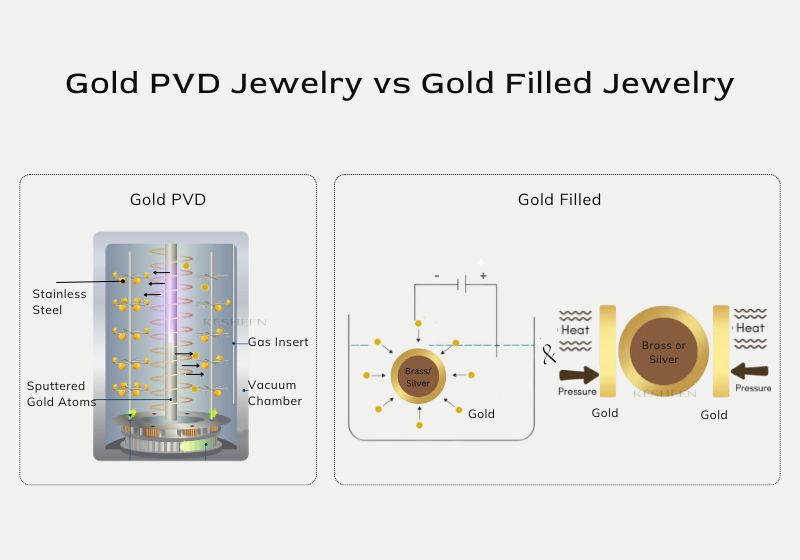
- Sputtering: In this technique, inert gas ions (typically argon) are accelerated towards the gold target. When these energetic ions strike the target, they knock off gold atoms, creating a cloud of gold vapor. The ionized gold atoms are then drawn towards the oppositely charged substrate.
- Arc Evaporation: Here, a high-current electric arc is struck on the surface of the gold target, creating a localized plasma hot spot. This intensely hot plasma rapidly evaporates and ionizes gold atoms from the target’s surface.
Both methods efficiently generate a highly reactive gold plasma or vapor, crucial for the subsequent deposition phase. The choice between sputtering and arc evaporation often depends on the specific application, desired film properties, and the type of equipment available.
Deposition and Film Growth
Once the gold atoms are vaporized and often ionized, they travel through the vacuum and condense onto the prepared substrate surface. The substrate itself may be heated to a specific temperature or held at an electrical bias to further optimize the deposition process. The ionized gold atoms, under the influence of an electric field, are accelerated towards the substrate, impacting it with significant energy. This high-energy impact facilitates the formation of a strong atomic bond between the gold and the substrate. The process allows for precise control over the film’s thickness, which can range from a few nanometers to several microns, depending on the application. The continuous bombardment and condensation build up a dense, uniform, and crystalline gold film layer by layer, resulting in the characteristic luster and enhanced durability.
Key Technological Benefits and Applications
The technical advantages of Gold PVD extend far beyond mere aesthetics, impacting product longevity, functionality, and manufacturing efficiency across various high-tech sectors.
Enhanced Durability and Performance
Gold PVD coatings are renowned for their exceptional hardness and wear resistance. The atomic-level bonding and dense film structure significantly increase the surface hardness of the underlying material, making it highly resistant to scratches, abrasions, and general wear and tear. This is particularly crucial for consumer electronics, luxury watches, and medical instruments that undergo frequent handling or exposure to harsh environments. Furthermore, the non-porous nature of PVD films offers superior corrosion resistance compared to electroplated coatings, forming an effective barrier against moisture, chemicals, and environmental degradation, thereby extending the lifespan of products.
Precision and Uniformity
One of the hallmarks of PVD technology is its capability for precision and uniformity. The vacuum deposition process allows for meticulous control over film thickness, often within nanometer tolerances, ensuring consistent performance and appearance across batches. This uniformity is vital for applications where precise electrical or optical properties are required. Additionally, PVD can coat complex geometries and internal surfaces with an even layer, a challenge for liquid-based processes where surface tension and gravity can lead to uneven distribution. This precision makes Gold PVD indispensable for miniaturized components and intricate designs found in modern gadgets.
Versatile Industrial Use Cases
The robust properties imparted by Gold PVD have led to its widespread adoption across a diverse array of industries:
- Consumer Electronics: Components in smartphones, wearables, and laptops benefit from durable, aesthetically pleasing gold finishes that resist wear.
- Luxury Goods: Watches, jewelry, and eyewear utilize Gold PVD for long-lasting, brilliant finishes that maintain their integrity for years.
- Medical Devices: Surgical instruments, implants, and diagnostic tools leverage the biocompatibility, corrosion resistance, and inertness of PVD gold.
- Aerospace and Automotive: Critical components require wear-resistant, anti-corrosive coatings that perform reliably under extreme conditions.
- Cutting Tools: Gold PVD is used to reduce friction and increase the lifespan of drills, mills, and other high-performance cutting tools.
- Optics: Gold PVD layers can create highly reflective and durable optical coatings for mirrors and sensors.
These applications underscore Gold PVD’s status as a versatile, high-performance coating technology essential for modern manufacturing.
Gold PVD in the Future of Manufacturing
The trajectory of Gold PVD technology points towards continuous innovation and broader integration within advanced manufacturing processes. Researchers are constantly exploring new material combinations, enhanced deposition techniques, and process optimizations to further improve film properties and reduce energy consumption. Advancements in plasma technology, real-time monitoring, and artificial intelligence are poised to make PVD even more precise, efficient, and adaptable. For example, hybrid PVD processes combining different deposition methods or integrating PVD with other surface treatments are emerging to create multi-functional coatings with unprecedented performance characteristics.
As industries increasingly demand materials with superior longevity, environmental responsibility, and complex functional properties, Gold PVD stands as a cornerstone technology. Its ability to create high-quality, durable, and aesthetically appealing gold surfaces without the ecological drawbacks of traditional methods ensures its pivotal role in the future of sustainable, high-performance product development. From the next generation of smart devices to mission-critical industrial components, Gold PVD will continue to define standards for advanced surface engineering.
aViewFromTheCave is a participant in the Amazon Services LLC Associates Program, an affiliate advertising program designed to provide a means for sites to earn advertising fees by advertising and linking to Amazon.com. Amazon, the Amazon logo, AmazonSupply, and the AmazonSupply logo are trademarks of Amazon.com, Inc. or its affiliates. As an Amazon Associate we earn affiliate commissions from qualifying purchases.