
In the modern landscape of high-performance computing, the pursuit of efficiency has driven engineers far beyond the capabilities of general-purpose processors. While a standard Central Processing Unit (CPU) or Graphics Processing Unit (GPU) can handle a vast array of tasks—from running operating systems to rendering complex 3D environments—their versatility comes at a cost: power inefficiency and slower execution speeds for highly specialized operations. Enter the Application Specific Integrated Circuit (ASIC), a specialized piece of silicon designed to perform one singular function, and to do it better, faster, and more efficiently than any general hardware ever could.

The Architectural Philosophy of ASICs
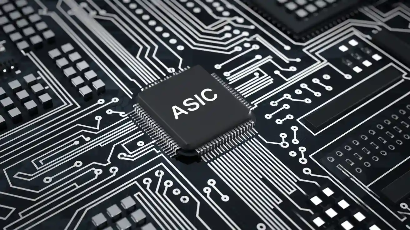
An ASIC is essentially a custom-built microchip. Unlike programmable hardware, such as Field-Programmable Gate Arrays (FPGAs) or standard CPUs that rely on firmware and software instructions to dictate logic, an ASIC’s logic is physically “hard-wired” into the silicon during the manufacturing process.
Hard-Wired Efficiency
The primary advantage of the ASIC is its architectural focus. When a chip is designed to run only one algorithm—for instance, the SHA-256 hashing algorithm used in Bitcoin mining—engineers can remove all the redundant circuitry required for general-purpose computing. There is no need for branch predictors, complex instruction decoders, or deep cache hierarchies that occupy space and consume power on a standard CPU. By stripping away everything unnecessary, the chip designer can pack significantly more processing elements into the same physical footprint.
Silicon Optimization and Throughput
Because the circuitry is purpose-built, the data path within an ASIC is optimized for the specific task at hand. Signals travel the shortest possible physical distance, and the logic gates are arranged to minimize latency. This leads to a massive increase in throughput. For many applications, an ASIC can perform trillions of operations per second while consuming only a fraction of the electricity required by a general-purpose processor attempting the same workload.
The Lifecycle and Development Process
Designing an ASIC is a high-stakes, capital-intensive endeavor. Unlike software development, where errors can be patched via an over-the-air update, an ASIC is immutable once it leaves the fabrication facility. If there is a design flaw, the entire batch of silicon is effectively useless, leading to millions of dollars in losses.
From RTL to GDSII
The process begins with Register Transfer Level (RTL) design, where engineers use Hardware Description Languages (HDL) like Verilog or VHDL to define how the chip should behave. Once the logic is simulated and verified, it undergoes synthesis, where the high-level design is mapped to actual physical logic gates. The final stage of the design phase is “Place and Route,” where the physical layout of the transistors and interconnects is determined. This output is a GDSII file, a complex roadmap sent to the semiconductor foundry.
The Fabrication Challenge
Fabricating an ASIC is one of the most complex industrial processes on the planet. It involves photolithography, etching, and thin-film deposition at the nanometer scale. Companies like TSMC, Samsung, and Intel are the primary players here, operating multi-billion dollar “fabs.” The cost of creating the “masks” (the stencils used to print the circuit onto the silicon) can run into the tens of millions of dollars before a single chip is even produced. This creates a high barrier to entry, meaning that ASIC development is usually reserved for products produced at massive scale, where the per-unit cost can be amortized across millions of chips.

Strategic Applications in Modern Tech
The utility of ASICs spans across several critical sectors. By shifting the workload from software to hardware, ASICs enable technologies that would otherwise be computationally prohibitive or thermally impossible to run on standard platforms.
Cryptocurrency Mining
The most visible application of ASICs in recent years has been in the cryptocurrency ecosystem. Bitcoin mining requires calculating SHA-256 hashes as fast as possible to secure the network and earn rewards. A general CPU is inefficient at this, and even high-end GPUs struggle to compete with the sheer hash-per-watt efficiency of an ASIC. Bitcoin mining has evolved into an arms race, where specialized ASIC miners are now the only viable hardware for professional-scale operations.
Artificial Intelligence and Machine Learning
Perhaps the most significant frontier for ASICs today is AI. Training large language models and running complex inference tasks requires performing billions of matrix multiplications. Tensor Processing Units (TPUs) and custom AI accelerators are specialized ASICs designed specifically for the heavy linear algebra required by neural networks. By optimizing hardware for floating-point math rather than general logic, companies like Google, NVIDIA, and various startups have drastically reduced the time required to train the AI models that define the current tech zeitgeist.
Networking and Consumer Electronics
Beyond mining and AI, ASICs are the unsung heroes of the digital infrastructure. Your home router, your smartphone’s image signal processor (ISP), and the massive switches that power the cloud all rely on ASICs. In networking, these chips handle packet forwarding and routing decisions at wire speed, ensuring that data moves across the internet without congestion. In consumer electronics, custom silicon handles tasks like video encoding, audio processing, and battery management, all while minimizing power consumption to keep your device slim and battery-efficient.
Comparing ASICs to the Alternatives
To understand why one would choose an ASIC, it is helpful to compare it against the alternatives: CPUs, GPUs, and FPGAs. Each represents a different point on the spectrum between flexibility and performance.
ASIC vs. FPGA: Flexibility vs. Efficiency
FPGAs are programmable chips. They allow a developer to change the hardware logic after the chip has been manufactured. This makes them ideal for prototyping or for applications where the algorithm might change over time. However, FPGAs are slower and more power-hungry than ASICs because they require a layer of programmable interconnects that add overhead. ASICs are the endgame—they are chosen when the algorithm is stable and the goal is maximum efficiency at the lowest unit cost.
The Trade-off of Generalization
The CPU remains the king of versatility. It is excellent at handling unpredictable, branching logic and diverse software environments. However, the “everything for everyone” approach is precisely what makes it inefficient for dedicated tasks. As we move further into the era of specialized computing, the future is not necessarily more powerful CPUs, but rather “heterogeneous computing”—a system where a general CPU manages the overall workflow, while a fleet of specialized ASICs handles the heavy lifting of specific tasks.
The Application Specific Integrated Circuit stands as a testament to the power of specialization. In an era where computational demands are scaling exponentially, the ability to build hardware that is perfectly aligned with its intended software mission is the ultimate competitive advantage. As we continue to push the boundaries of AI, global networking, and data processing, the ASIC will remain the silent, high-speed engine driving the next generation of technological innovation.
aViewFromTheCave is a participant in the Amazon Services LLC Associates Program, an affiliate advertising program designed to provide a means for sites to earn advertising fees by advertising and linking to Amazon.com. Amazon, the Amazon logo, AmazonSupply, and the AmazonSupply logo are trademarks of Amazon.com, Inc. or its affiliates. As an Amazon Associate we earn affiliate commissions from qualifying purchases.