
In the realm of computer architecture, the central processing unit (CPU) is often heralded as the “brain” of the machine, while the hard drive is seen as its long-term memory. However, even the fastest processor in the world would be useless if it had no way to communicate with other components. This is where the “bus” comes into play. A computer bus is a communication system that transfers data between components inside a computer, or between computers themselves. If the CPU is the brain, the bus system is the central nervous system, providing the high-speed pathways necessary for instructions and data to reach their destinations.

Understanding the intricacies of computer buses is essential for anyone looking to grasp how hardware performance scales, how peripherals interact with the motherboard, and how modern innovations like NVMe storage and high-end GPUs achieve their staggering speeds.
The Fundamental Architecture of Computer Buses
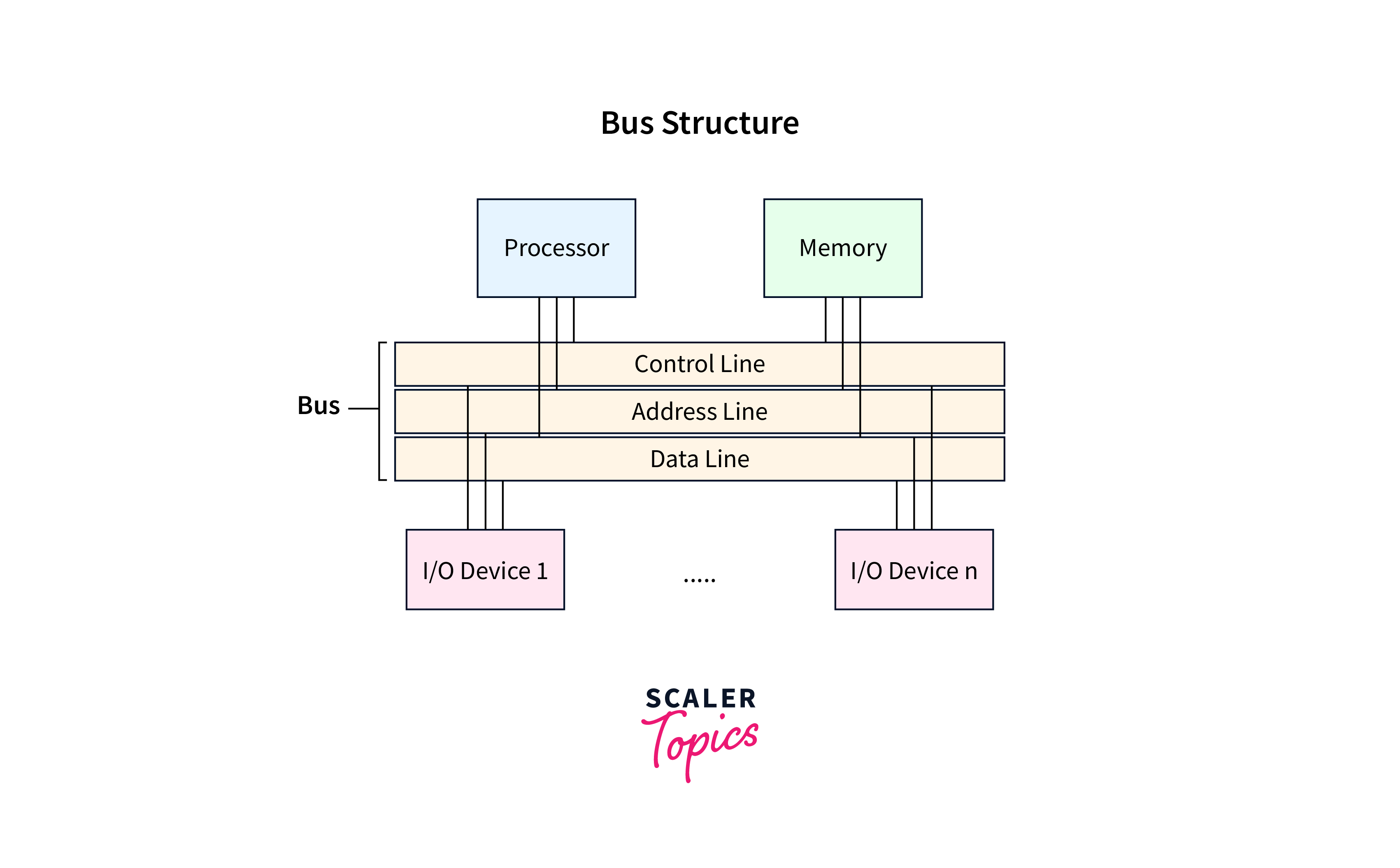
A computer bus is more than just a set of wires; it is a sophisticated logical and physical interface governed by strict protocols. In early computing, buses were literally bundles of wire connecting various components, but modern systems utilize complex integrated circuits and printed circuit board (PCB) traces. To understand how a bus works, we must look at its three primary functional components: the Data Bus, the Address Bus, and the Control Bus.
The Data Bus
The data bus is perhaps the most critical component for end-user performance. Its primary responsibility is to carry the actual information—the bits and bytes—between the CPU, memory, and input/output (I/O) devices. The “width” of the data bus is a key factor in determining a computer’s processing power. A 64-bit data bus can move 64 bits of data simultaneously. Think of this as the number of lanes on a highway; the more lanes you have, the more vehicles (data) can travel at the same time without causing a bottleneck.
The Address Bus
Before data can be transferred, the system must know where that data is going or where it is coming from. The address bus is used by the CPU to specify a physical address in the system memory. When the CPU needs to read or write data to a specific location in RAM, it sends the address of that location through the address bus. The width of the address bus determines the maximum amount of memory the system can reference. For example, a 32-bit address bus can address $2^{32}$ locations, which limits the system to 4GB of RAM—a limitation that led to the universal adoption of 64-bit architectures in modern computing.
The Control Bus
The control bus is the management layer of the system. It carries signals that report the status of various devices and coordinate the timing of data transfers. It transmits commands like “read” or “write” and carries interrupt signals from hardware components. Without the control bus, the data and address buses would be chaotic; the control bus ensures that the CPU and peripherals are synchronized and that data is not sent to a device that isn’t ready to receive it.
Internal vs. External Buses: Connecting the Ecosystem
Computer buses are generally categorized based on their location and role within the system. The two primary types are internal (system) buses and external (expansion) buses.
The System Bus (Internal Bus)
The system bus connects the most vital internal components: the CPU and the main memory (RAM). In older architectures, this was often referred to as the Front Side Bus (FSB). The speed of the system bus is a massive determinant of overall system responsiveness. If the CPU can process data faster than the system bus can deliver it from RAM, the CPU must enter “wait states,” wasting valuable clock cycles. In modern systems, the traditional FSB has been replaced by more efficient point-to-point interconnects, such as Intel’s QuickPath Interconnect (QPI) or AMD’s Infinity Fabric, which allow for much higher throughput and lower latency.
Expansion Buses (External Bus)
Expansion buses allow the computer to interact with the outside world and specialized hardware. These are the pathways that connect the motherboard to peripherals like graphics cards, sound cards, USB drives, and network adapters.
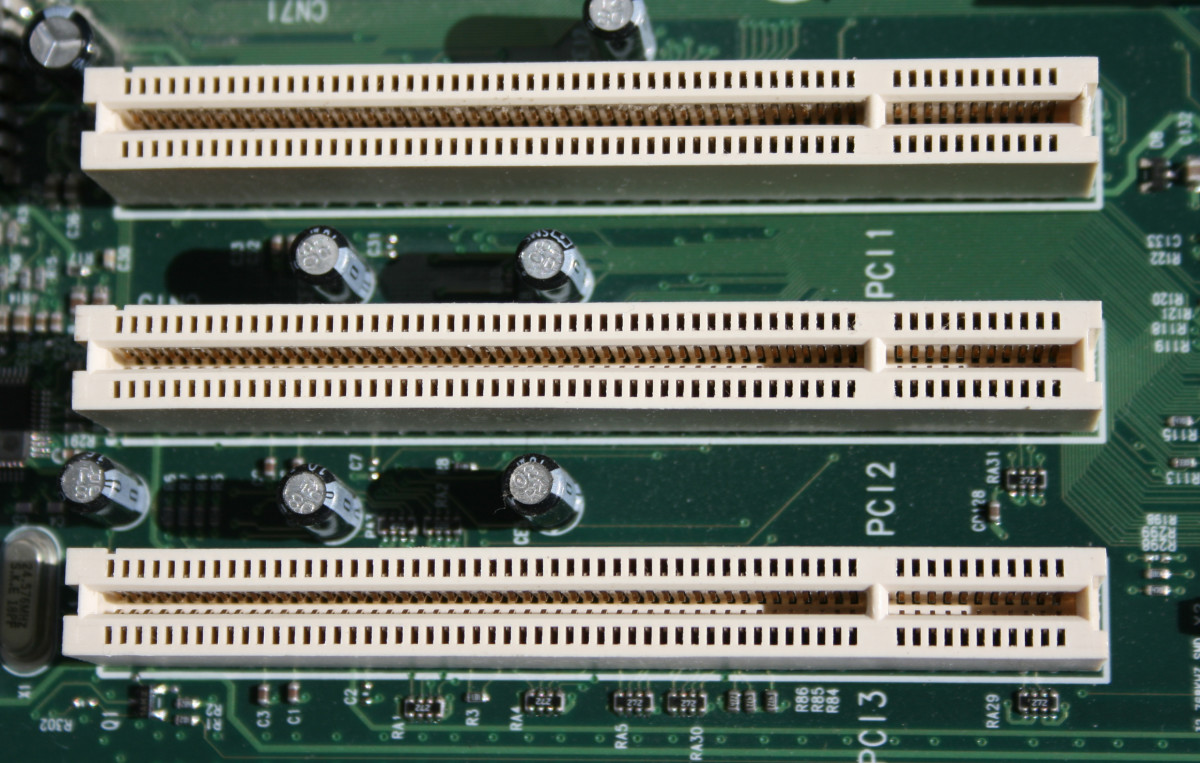
The history of expansion buses is a history of increasing bandwidth demands. We have moved from the slow ISA (Industry Standard Architecture) slots of the 1980s to the ubiquitous PCI (Peripheral Component Interconnect) in the 1990s, and finally to the modern PCIe (PCI Express) standard. Unlike the shared parallel bus architecture of the original PCI, PCIe uses a high-speed serial point-to-point architecture, which allows each connected device to have its own dedicated connection to the chipset or CPU, preventing devices from competing for bandwidth.
From Parallel to Serial: The Great Evolution of Data Transfer
One of the most significant shifts in computer bus technology has been the transition from parallel communication to serial communication. On the surface, this seems counterintuitive. A parallel bus sends multiple bits of data simultaneously across multiple wires, while a serial bus sends bits one after another over a single pair of wires. Logic would suggest that parallel is faster, but as clock speeds increased, physics presented a major obstacle: “clock skew.”
Why Parallel Isn’t Always Faster
In a parallel bus, all bits in a byte must arrive at the destination at exactly the same time. At high speeds, electromagnetic interference and slight differences in the length of the wires cause some bits to arrive slightly later than others. This “skew” forces the system to wait for the slowest bit, effectively capping the speed of parallel buses.
The Rise of High-Speed Serial Buses
Modern standards like USB (Universal Serial Bus), SATA, and PCIe solved this by using high-speed serial communication. By sending data extremely fast over fewer wires and using sophisticated encoding schemes, serial buses can achieve frequencies that would be impossible for parallel buses. This evolution is what allowed us to move from the bulky 40-pin IDE cables of the past to the slim, high-speed SATA cables and the incredibly fast M.2 NVMe slots we use today.
Modern High-Performance Buses: PCIe 5.0, NVMe, and CXL
As we move into an era of 4K video editing, real-time ray tracing, and massive data sets, the demand on the computer bus has never been higher. Today, the focus is on maximizing throughput and minimizing “bottlenecks.”
PCI Express (PCIe) Lanes
The modern gold standard for expansion is PCIe. It is measured in “lanes” (x1, x4, x8, x16). Each lane consists of two pairs of wires—one for transmitting and one for receiving. A modern graphics card typically uses a PCIe x16 slot, providing 16 dedicated lanes for data transfer. With the arrival of PCIe 5.0, the bandwidth has doubled over the previous generation, reaching up to 64 GB/s in an x16 configuration. This headroom is vital for high-end GPUs and enterprise-grade networking equipment.
NVMe and the Storage Revolution
The transition from the SATA bus to the NVMe (Non-Volatile Memory express) protocol is perhaps the most noticeable “bus” upgrade for the average user. SATA was originally designed for spinning hard drives and was limited by its AHCI protocol. NVMe, however, allows SSDs to connect directly to the PCIe bus. By bypassing the old controller bottlenecks and utilizing the high-speed lanes of the PCIe bus, NVMe drives can achieve read/write speeds that are ten to twenty times faster than traditional SATA SSDs.
Compute Express Link (CXL)
In the world of data centers and high-performance computing (HPC), a new bus standard called CXL is gaining traction. Built on the physical foundation of PCIe 5.0, CXL allows for high-speed, low-latency communication between the CPU and specialized accelerators like GPUs or AI processors. Crucially, CXL supports “memory coherency,” meaning the CPU and the accelerator can share the same memory space efficiently, reducing the need to constantly copy data back and forth.
The Role of Buses in the Future of Computing and AI
As we look toward the future, the computer bus is evolving to meet the unique challenges of Artificial Intelligence (AI) and machine learning. AI workloads require the movement of massive amounts of data between memory and processing units. Standard bus architectures are often the primary limiting factor in AI training speeds, a phenomenon known as the “Memory Wall.”
To combat this, manufacturers are developing proprietary, ultra-high-speed interconnects. NVIDIA’s NVLink is a prime example; it is a high-bandwidth bus that allows GPUs to communicate with each other at speeds far exceeding standard PCIe. This allows multiple GPUs to act as a single, massive processor.
Furthermore, the integration of HBM (High Bandwidth Memory) directly onto the processor package represents a shift in bus philosophy. By placing the memory as close to the processor as possible and using thousands of microscopic “micro-bumps” to create an incredibly wide bus, manufacturers can achieve bandwidths in the terabytes-per-second range.
In conclusion, the computer bus is far more than a passive set of wires. It is a dynamic and essential component of computer science that dictates the limits of what hardware can achieve. From the humble 8-bit buses of the early computing era to the lightning-fast PCIe 5.0 lanes of today, the evolution of the bus has been a journey of overcoming physical limitations to keep pace with the ever-increasing speed of the CPU. As we move into an era defined by AI and exascale computing, the innovation within bus architecture will continue to be the silent engine driving the next generation of technological breakthroughs.
aViewFromTheCave is a participant in the Amazon Services LLC Associates Program, an affiliate advertising program designed to provide a means for sites to earn advertising fees by advertising and linking to Amazon.com. Amazon, the Amazon logo, AmazonSupply, and the AmazonSupply logo are trademarks of Amazon.com, Inc. or its affiliates. As an Amazon Associate we earn affiliate commissions from qualifying purchases.