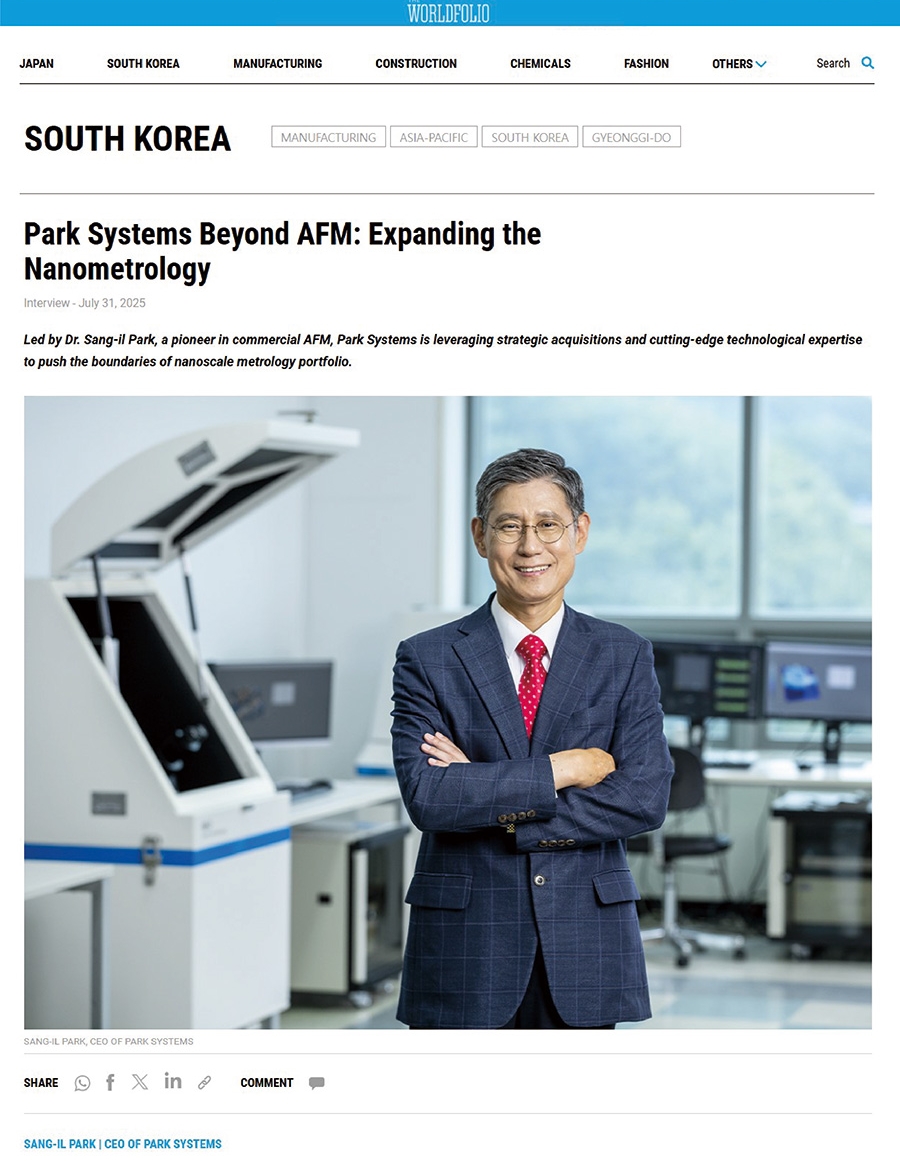
Park Systems, a name that has steadily risen in prominence within the global scientific instrumentation landscape, is a South Korean company dedicated to pushing the boundaries of nanoscale analysis. While the term “systems” might evoke images of broad technological infrastructure, Park Systems’ focus is intensely specific: atomic force microscopy (AFM). They are not a general technology conglomerate, nor primarily a brand consultancy or a financial entity. Instead, their core competency lies squarely within the realm of Tech, specifically in the development, manufacturing, and distribution of cutting-edge AFM instrumentation. This niche allows them to serve a diverse clientele ranging from academic researchers and industrial R&D departments to quality control laboratories and advanced manufacturing facilities. Their contribution to the technological ecosystem is significant, enabling scientists and engineers to observe, measure, and manipulate matter at the atomic and molecular levels, a feat previously unimaginable.
![]()
The Power of Atomic Force Microscopy: Unveiling the Nanoscale World
Atomic Force Microscopy (AFM) represents a paradigm shift in our ability to visualize and characterize materials. Unlike traditional optical microscopes, which rely on light to form images, AFM operates by scanning a sharp tip across a sample’s surface. This tip, often just a few atoms wide, interacts with the surface through interatomic forces. By precisely measuring the deflection of a laser beam reflected off the back of the cantilever holding the tip, an incredibly detailed three-dimensional topographical map of the surface can be generated. This technique is revolutionary because it doesn’t require samples to be conductive (a limitation of electron microscopy) and can be performed in various environments, including air, liquids, and vacuum. This versatility opens up applications in a vast array of fields, from semiconductor manufacturing and advanced materials research to biological sciences and nanotechnology. Park Systems has positioned itself as a leader in advancing this powerful technology, making it more accessible, more precise, and more versatile than ever before.
Fundamental Principles of AFM Operation
At its heart, AFM relies on the delicate interplay between a sharp probe and the sample surface. The probe, typically a silicon or silicon nitride tip mounted on a flexible beam called a cantilever, is brought into close proximity with the surface. As the tip encounters the contours of the surface, it experiences forces – van der Waals forces, electrostatic forces, magnetic forces, and others – depending on the specific tip and sample. These forces cause the cantilever to bend or deflect. A laser beam is precisely focused on the back of the cantilever, and its reflection is directed onto a photodetector. As the cantilever deflects, the position of the reflected laser beam on the photodetector changes, which is then translated into a signal representing the tip’s vertical displacement. A piezoelectric scanner then precisely moves the tip or the sample in the x, y, and z directions, allowing the tip to traverse the entire surface and build a comprehensive topographical image. The resolution achievable with AFM can be as high as nanometers or even angstroms, providing unprecedented detail about surface features.
Diverse Imaging Modes for Comprehensive Analysis
The true power of AFM lies in its ability to operate in various modes, each designed to extract different types of information about the sample. Park Systems meticulously engineers their instruments to support a wide spectrum of these modes, catering to diverse analytical needs.
Topographical Imaging: The Foundation of AFM
The most fundamental mode is contact mode, where the tip is in constant contact with the sample surface. While simple and fast, it can potentially damage soft samples and wear down the tip. To mitigate this, tapping mode (also known as intermittent contact mode) became popular. Here, the cantilever is oscillated at its resonant frequency, and the tip intermittently “taps” the surface. This significantly reduces lateral forces, preserving delicate sample structures and prolonging tip life. These modes are crucial for understanding surface roughness, identifying defects, and characterizing microstructures.
Beyond Topography: Exploring Material Properties
AFM’s capabilities extend far beyond simply mapping height. Park Systems’ instruments enable advanced modes that probe various material properties. Phase imaging, for instance, is sensitive to variations in the energy lost during the tip-sample interaction, revealing differences in material composition, adhesion, and viscoelasticity. This is invaluable for characterizing complex polymer blends, biological membranes, and composite materials.
Force spectroscopy is another critical application. Here, the tip is brought into contact with a specific point on the surface and then retracted, measuring the force as a function of distance. This allows for the determination of mechanical properties like Young’s modulus, adhesion forces, and the unfolding of individual biomolecules. This has profound implications in biophysics and materials science for understanding the mechanical behavior of cells, proteins, and nanoscale structures.
Furthermore, advanced functionalities include electrical and magnetic characterization. Techniques like Conductive AFM (C-AFM) measure the current flowing between the tip and the sample, enabling the mapping of conductivity variations at the nanoscale. Magnetic Force Microscopy (MFM) uses a magnetic tip to detect and map magnetic fields emanating from the sample, crucial for studying magnetic storage media and spintronic devices. Park Systems’ commitment to providing a comprehensive suite of imaging modes ensures that researchers can perform in-depth, multi-faceted analyses of their samples.
Park Systems’ Technological Innovations: Driving AFM Advancement
Park Systems is not merely a manufacturer of AFM instruments; they are innovators, consistently pushing the envelope of what’s possible at the nanoscale. Their dedication to research and development has resulted in several key technological advancements that distinguish their products and enhance the user experience and analytical capabilities. This commitment to innovation is central to their identity as a leading tech company in the scientific instrumentation sector.
Precision Engineering for Unparalleled Resolution and Stability
The accuracy and reliability of AFM data are directly tied to the precision of the instrument’s components. Park Systems invests heavily in engineering excellence, ensuring every aspect of their AFMs, from the scanner and tip mechanics to the environmental control systems, is designed for optimal performance.
Advanced Scanner Technology: The Heart of Motion Control
The piezoelectric scanner is the component responsible for precise movement of the tip or sample across the surface. Park Systems has developed highly sophisticated scanner designs that offer exceptional linearity, repeatability, and a large scanning range. This ensures that even subtle surface features are accurately captured and that large areas can be mapped without compromising resolution. The stability of these scanners is paramount for long-term measurements and for achieving the highest possible resolution. Their designs often incorporate closed-loop control systems, which use sensors to constantly monitor and correct for any deviations in movement, guaranteeing unparalleled precision.
Tip-Sample Interaction Optimization: Enhancing Data Quality
The interaction between the AFM tip and the sample surface is the cornerstone of AFM operation. Park Systems focuses on optimizing this interaction through various means. This includes developing highly stable cantilever holders, precise tip positioning systems, and sophisticated feedback loops that maintain optimal tip-sample engagement. By minimizing external vibrations and electrical noise, they ensure that the subtle forces being measured are accurately translated into meaningful data. Their commitment to minimizing artifacts and maximizing signal-to-noise ratio is what allows researchers to obtain the most reliable and insightful nanoscale images and measurements.
User-Centric Design and Intelligent Software Solutions
Beyond the hardware, Park Systems places a strong emphasis on making their powerful AFM technology accessible and user-friendly. This is achieved through intuitive software interfaces and intelligent automation features that streamline the entire workflow.
Intuitive Software Interfaces: Simplifying Complex Operations
Operating an AFM can be complex, requiring a deep understanding of various parameters and imaging modes. Park Systems has developed software that simplifies this process significantly. Their user interfaces are designed to be intuitive and logically laid out, guiding users through setup, data acquisition, and analysis. This allows researchers, regardless of their prior AFM experience, to quickly become proficient and obtain high-quality data. Features such as automated tip calibration, real-time image feedback, and pre-set measurement protocols contribute to a more efficient and less daunting user experience.
Intelligent Automation and AI Integration: Accelerating Discovery
Recognizing the growing demand for faster and more efficient research, Park Systems has been at the forefront of integrating intelligent automation and even early forms of AI into their AFM systems. This includes automated sample positioning, automated parameter optimization for different imaging modes, and AI-powered image analysis tools that can identify and quantify features of interest with minimal user intervention. These features not only speed up experiments but also help to reduce human error and enable researchers to focus on interpreting the scientific insights rather than the operational minutiae. This forward-looking approach underscores their position as a technology leader.
Applications Across Diverse Scientific and Industrial Sectors
The impact of Park Systems’ advanced AFM technology reverberates across a broad spectrum of scientific disciplines and industrial applications. By providing tools that enable the precise characterization of materials at the nanoscale, they empower innovation and problem-solving in fields that are critical to technological advancement and human well-being. Their instruments are not confined to academic ivory towers; they are integral to the development and manufacturing processes of cutting-edge industries.
Advancing Materials Science and Nanotechnology Research
The ability to observe and manipulate matter at the atomic and molecular level is fundamental to the advancement of materials science and nanotechnology. Park Systems’ AFMs are indispensable tools for researchers exploring new materials with novel properties and for understanding the fundamental behaviors of nanoscale structures.
Characterizing Novel Nanomaterials: From Graphene to Quantum Dots
The discovery and development of new nanomaterials, such as graphene, carbon nanotubes, and quantum dots, have been heavily reliant on advanced microscopy techniques. AFM allows for the direct visualization of these materials’ unique structures, the characterization of their surface morphology, and the measurement of their mechanical and electrical properties at the nanoscale. Researchers use Park Systems’ AFMs to assess the quality of synthesized nanomaterials, identify defects, and understand how their structure influences their performance in various applications, from advanced electronics to next-generation sensors.
Understanding Surface Interactions and Thin Film Deposition
In many advanced technologies, the properties of surfaces and thin films are paramount. AFM is crucial for studying surface roughness, adhesion, and wear of thin films used in coatings, microelectronics, and biomedical devices. Park Systems’ instruments enable scientists to meticulously analyze the growth mechanisms of thin films during deposition processes, understand interfacial phenomena, and optimize film properties for specific applications. This is vital for developing more durable, efficient, and functional materials.
Revolutionizing Biological and Biomedical Research
The biological world operates at the nanoscale, making AFM an exceptionally powerful tool for life sciences. Park Systems’ AFMs are used to study the structure, function, and interactions of biological molecules and systems with unprecedented detail.
Visualizing and Manipulating Biomolecules: Proteins, DNA, and Cells
AFM allows researchers to directly image and even manipulate individual biomolecules like proteins and DNA. This enables the study of their conformational changes, binding interactions, and mechanical properties. For example, researchers can unfold single protein molecules to understand their folding pathways and stability, or observe the assembly of DNA nanostructures. Furthermore, AFM can be used to study the surface topography and mechanical properties of living cells, providing insights into cellular mechanics, membrane dynamics, and the effects of drugs or environmental stimuli.
Advancements in Medical Diagnostics and Drug Delivery
The precision offered by AFM has significant implications for the development of new medical diagnostics and drug delivery systems. Researchers are using AFM to characterize the surfaces of implants and biosensors, ensuring biocompatibility and optimal performance. In drug delivery, AFM can be employed to study the encapsulation efficiency and release profiles of nanoparticles and liposomes, crucial for designing effective and targeted therapies. The ability to analyze these systems at the nanoscale ensures the development of safer and more efficacious medical technologies.
Enabling Quality Control and Manufacturing in High-Tech Industries
Beyond fundamental research, Park Systems’ AFMs play a critical role in ensuring the quality and driving innovation in high-tech manufacturing sectors, particularly in semiconductors and advanced electronics.
Semiconductor Wafer Inspection and Defect Analysis
The semiconductor industry relies on meticulously precise manufacturing processes, where even microscopic defects can render entire batches of chips unusable. Park Systems’ AFMs are widely used for non-destructive wafer inspection, allowing engineers to detect and characterize minute surface defects, contamination, and structural anomalies that are invisible to optical inspection methods. This early detection of flaws significantly reduces manufacturing costs and improves yield. Their ability to operate in cleanroom environments and provide high-resolution topographical data makes them an indispensable part of the semiconductor QC workflow.
Characterization of Advanced Electronic Components and Displays
The development of next-generation electronic devices, including flexible displays, advanced sensors, and micro-electro-mechanical systems (MEMS), requires detailed characterization of their nanoscale features. AFM provides the necessary resolution to inspect the uniformity of conductive layers, the surface topography of micro-patterned components, and the integrity of insulating layers. This enables manufacturers to optimize their designs, identify failure mechanisms, and ensure the reliability and performance of these sophisticated electronic products. Park Systems’ commitment to providing robust and versatile AFM solutions makes them a key partner for innovation in these rapidly evolving industries.
aViewFromTheCave is a participant in the Amazon Services LLC Associates Program, an affiliate advertising program designed to provide a means for sites to earn advertising fees by advertising and linking to Amazon.com. Amazon, the Amazon logo, AmazonSupply, and the AmazonSupply logo are trademarks of Amazon.com, Inc. or its affiliates. As an Amazon Associate we earn affiliate commissions from qualifying purchases.