In the fast-paced world of technology, where we often focus on the sleek glass of a smartphone or the invisible architecture of a neural network, it is easy to forget the physical elements that make modern computing possible. At the heart of this digital revolution lies a metal that has been used by humanity for millennia: copper. However, to the modern tech engineer, data center architect, or hardware enthusiast, “raw copper” is much more than a shiny penny.
Understanding what raw copper looks like—and how its physical state evolves through various stages of technological refinement—is essential for understanding the backbone of our global infrastructure. From the jagged, dull ores extracted from the earth to the hyper-pure, mirror-finish foils used in semiconductor packaging, the visual journey of copper is a story of technological triumph.

The Elemental Aesthetic: Visual Characteristics of Copper Ore and Refined Metal
To understand what raw copper looks like, one must first distinguish between “native copper” and the copper ores that are most commonly found in nature. Unlike gold, which often appears in the earth as brilliant yellow nuggets, copper is a reactive element that frequently hides its true identity behind layers of oxidation and mineral complexity.
The Appearance of Native Copper and Ores
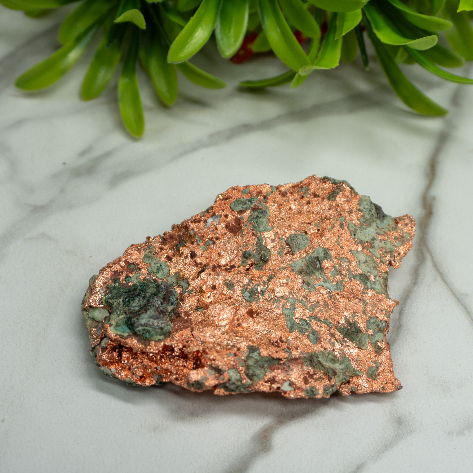
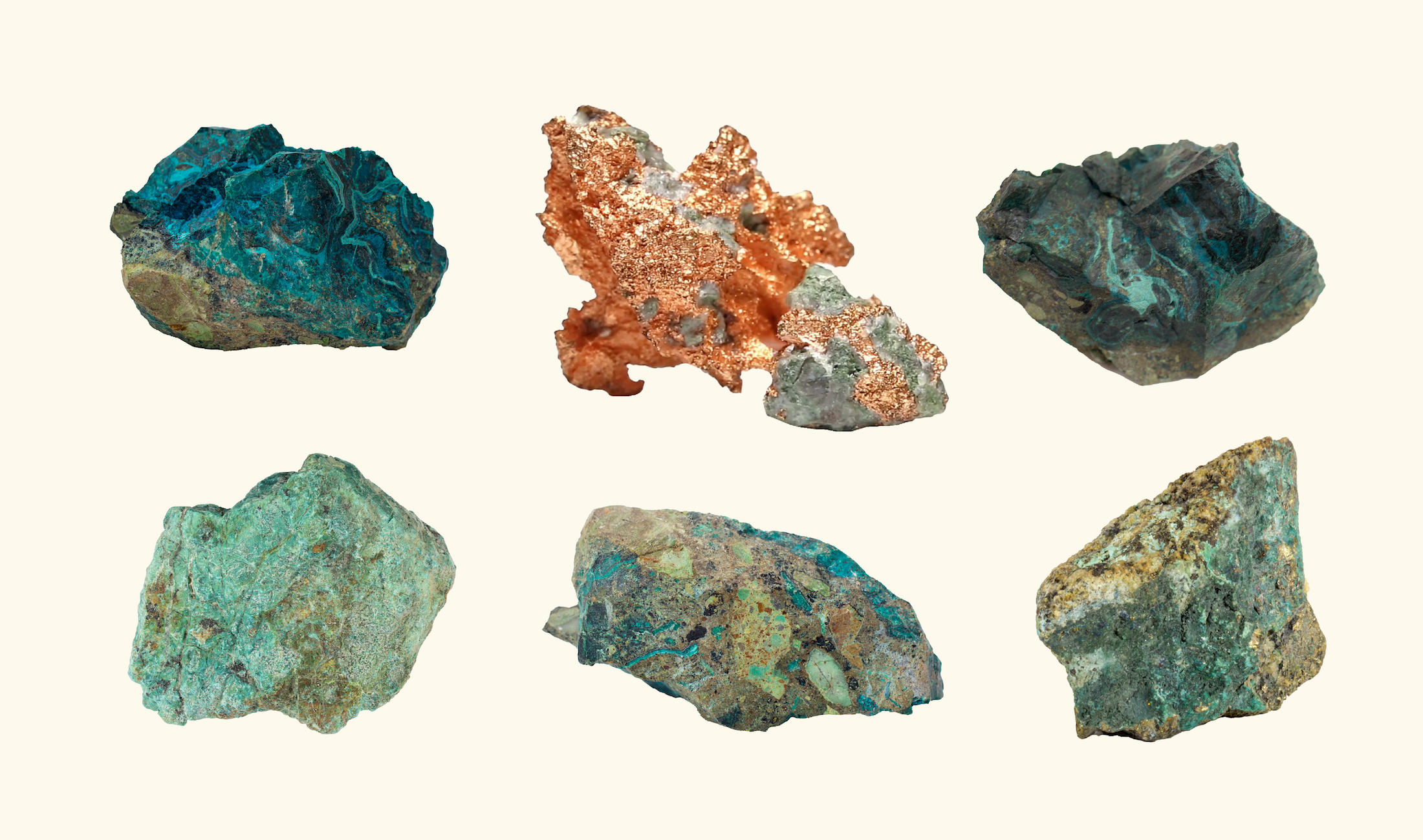
In its rarest natural form, known as native copper, the metal appears as irregular, dendritic (branch-like) masses. It has a distinct reddish-orange or “salmon-pink” hue on a freshly broken surface. However, because copper reacts with oxygen, these natural specimens are often coated in a dark, dull brown or black layer of copper oxide.
Most industrial copper used in technology starts its life as ore, such as Chalcopyrite or Malachite. Chalcopyrite often looks like “fool’s gold”—a brassy, metallic yellow—while Malachite is famous for its vibrant, silky green bands. For a tech manufacturer, these colorful rocks are the rawest form of the conductive pathways that will eventually power a high-end GPU.
The Refinement Transition: From Blister to Cathode
Once processed, the copper undergoes a metamorphosis. “Blister copper,” which is about 98% pure, has a blistered, uneven surface caused by escaping gases during the smelting process. It looks rugged, gray-black, and unrefined.
The true “tech-ready” raw state is the copper cathode. These are large, flat sheets produced via electrowinning. In this state, the copper looks remarkably pure, possessing a soft, matte metallic luster with a consistent peach-to-pink coloration. This is the starting point for the high-purity applications required in digital security hardware and advanced circuitry.
Copper in the Silicon Age: Why the “Look” of High-Purity Copper Matters for Electronics
As we move from the mine to the fabrication plant (fab), the appearance of copper changes as it is manipulated at the microscopic level. In the tech industry, the visual uniformity of copper is a direct indicator of its conductive efficiency and reliability.
The Microscopic Landscape of Interconnects
In modern semiconductor manufacturing, copper is used for “interconnects”—the tiny wires that link transistors on a chip. When viewed under an electron microscope, raw copper deposited via physical vapor deposition (PVD) looks like a dense, crystalline landscape. At this scale, any “impurity” or visual irregularity can lead to electromigration, a phenomenon where atoms move under the influence of an electric current, potentially causing a device to fail.
The “look” of the copper here is judged by its grain structure. Tech engineers strive for a uniform, tightly packed grain to ensure that signals move at the speed of light without resistance. This is the “hidden” raw copper that defines the performance of the latest AI accelerators and processors.
Electroplating and the Mirror Finish
For Printed Circuit Boards (PCBs), copper is often applied through electroplating. Raw copper used in this context must look perfectly smooth. Any pits, nodules, or “orange peel” textures on the surface of the copper foil can interfere with high-frequency signals. In the world of 5G technology and high-speed data transmission, the copper must possess a “mirror-like” finish to minimize “skin effect” losses, where the current flows primarily on the surface of the conductor.
The Industrial Evolution: From Raw Nugget to Thermal Management Solutions
Beyond its role as a conductor of electricity, copper’s visual and physical properties make it the gold standard for thermal management in the tech world. If you have ever opened a high-performance gaming laptop or a server blade, you have seen the distinctive glow of raw copper heat pipes.
The Aesthetics of Heat Pipes and Vapor Chambers
In thermal design, raw copper is often drawn into hollow pipes or pressed into flat vapor chambers. In this application, the copper is typically left unplated to maximize its thermal emissivity. It possesses a bright, metallic sheen that transitions into a deep amber over time as it undergoes thermal cycling.
The internal structure of these components is where the “tech” happens. Inside a copper heat pipe is a “wick” structure, often made of sintered copper powder. This “raw” powder looks like fine, reddish-orange sand. This porous texture allows for the capillary action that moves liquid coolant, keeping high-end CPUs from melting under the load of complex AI workloads.
Copper in Data Center Infrastructure
On a macro scale, the “look” of copper defines the aesthetics of the modern data center. Massive busbars—thick, solid rectangular bars of raw copper—carry enormous amounts of current to server racks. These bars are often polished to a high shine to ensure a low-resistance contact point. The sight of these heavy, gleaming orange-gold pillars against the cold, sterile blue of a server room is a testament to the metal’s enduring importance in the digital age.
The Future of Copper Tech: Sustainability, Recycling, and Digital Security
As the demand for copper skyrockets due to the transition to Electric Vehicles (EVs) and the expansion of AI infrastructure, the way we perceive “raw copper” is shifting toward a circular economy. The look of “new” copper is increasingly being replaced by the look of “recycled” copper.
The “Urban Mine” and Recycled Aesthetics
Raw copper today is just as likely to come from an “urban mine”—recycled e-waste—as it is from a traditional pit mine. Recycled copper, once melted down and re-refined, is indistinguishable from virgin copper. However, the process of getting there involves sorting through “shred,” which is a chaotic mix of chopped wires, green PCB fragments, and multicolored insulation.
For tech companies focused on ESG (Environmental, Social, and Governance) goals, the ability to trace copper back to its raw origins is becoming a digital security and branding requirement. Blockchain technology is now being used to create “digital passports” for copper batches, ensuring that the raw metal used in a specific batch of laptops was sourced ethically and sustainably.
Synthetic Copper and Nano-Materials
Looking forward, we are seeing the emergence of copper-based nanomaterials. These “synthetic” versions of raw copper don’t look like metal at all; they often appear as dark, opaque inks or suspended colloidal liquids. These copper inks allow for “printed electronics,” where conductive pathways can be inkjet-printed onto flexible surfaces. This represents the ultimate evolution of what raw copper can “look like”—from a heavy, solid mineral to a fluid, digital-ready medium.
Conclusion: The Red Metal’s Enduring Tech Legacy
What does raw copper look like? It looks like the past, present, and future of human ingenuity. It is the dull green of the unmined earth, the vibrant pink of the refined cathode, the mirror-finish of the high-speed circuit, and the amber glow of the cooling system.
In the technology sector, copper is far more than a commodity. Its visual properties—its luster, its grain, and its oxidation state—are vital indicators of the health and efficiency of our digital world. As we push toward more powerful AI, faster connectivity, and a greener planet, the “look” of raw copper will continue to evolve, remaining the essential, colorful thread that connects our physical reality to our digital aspirations. For the tech professional, seeing the beauty in raw copper is about recognizing the raw potential of the machines that define our lives.
aViewFromTheCave is a participant in the Amazon Services LLC Associates Program, an affiliate advertising program designed to provide a means for sites to earn advertising fees by advertising and linking to Amazon.com. Amazon, the Amazon logo, AmazonSupply, and the AmazonSupply logo are trademarks of Amazon.com, Inc. or its affiliates. As an Amazon Associate we earn affiliate commissions from qualifying purchases.