In the vast lexicon of scientific terms, “deposition” might initially conjure images of geological processes or legal proceedings. However, within the realms of chemistry, physics, and materials science, deposition refers to a fundamental phase transition where a substance changes directly from a gaseous state to a solid state without first passing through a liquid phase. This fascinating phenomenon is the reverse of sublimation and plays a critical, often unseen, role in countless natural processes and, perhaps more surprisingly, underpins much of the advanced technology that defines our modern world. From the intricate circuits in your smartphone to the protective coatings on aerospace components, the controlled application of scientific deposition techniques is a cornerstone of innovation, directly impacting technology, economic value, and even brand perception.
The Fundamental Science of Deposition
To truly grasp the significance of deposition, we must first delve into its core scientific principles. It’s more than just a simple change of state; it’s a thermodynamically driven process with profound implications.
What is Deposition? A Phase Transition Defined
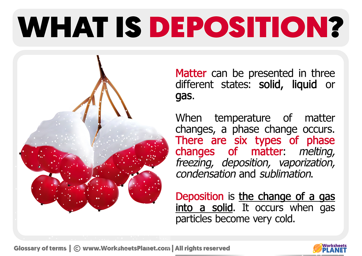
At its heart, deposition is a phase change, similar to freezing (liquid to solid) or condensation (gas to liquid). However, its uniqueness lies in bypassing the liquid phase entirely. Imagine water vapor in the atmosphere. Under specific conditions, instead of forming liquid raindrops (condensation), it can directly crystalize into solid ice, forming frost on a cold morning or snowflakes high in the clouds. This direct gas-to-solid transition is precisely what deposition is.
From a molecular perspective, individual gas molecules (atoms, ions, or compounds) possess significant kinetic energy, allowing them to move freely and independently. When these gas molecules encounter a cooler surface or environment, they lose energy. If the energy loss is sufficient and rapid enough, and the conditions preclude the formation of a liquid phase (often due to low pressure or specific temperature ranges), these molecules will bond directly with the surface, forming a solid layer or crystal structure. This process is exothermic, meaning it releases energy, often in the form of heat, as the molecules settle into a more ordered, lower-energy solid state. The reverse process, sublimation, requires energy input to break these solid bonds and release molecules into a gas. Understanding this fundamental energy exchange is crucial for controlling deposition processes in industrial applications.
Mechanisms and Driving Forces
The successful formation of a solid layer through deposition isn’t merely a matter of cooling a gas. It involves a complex interplay of physical and chemical mechanisms influenced by several critical factors. The journey from a dispersed gas to a cohesive solid typically follows two main stages:
- Nucleation: This is the initial formation of tiny, stable solid clusters (nuclei) on the substrate surface. Gas molecules collide with the surface, adhere (adsorption), and then move around until they find other adsorbed molecules to bond with, forming stable islands. The rate of nucleation depends heavily on the substrate material, its surface energy, temperature, and the concentration of the gas species. A “clean” and appropriate surface is often vital to promote uniform nucleation.
- Growth: Once nuclei have formed, additional gas molecules continue to deposit onto these existing clusters, causing them to expand and eventually coalesce into a continuous film or a larger crystal. The growth phase is influenced by the rate at which new gas molecules arrive at the surface, their mobility on the surface, and their ability to incorporate into the growing solid structure.
Key driving forces and parameters that control these mechanisms include:
- Temperature: Substrate temperature critically affects both nucleation and growth. Too cold, and molecules might not have enough mobility to find optimal bonding sites, leading to amorphous or disordered films. Too hot, and molecules might desorb before stable bonding occurs.
- Pressure: The partial pressure of the gas being deposited influences the rate at which molecules arrive at the surface. Higher pressures generally mean higher deposition rates, though this can also affect film quality and purity.
- Precursor Material: The chemical nature of the gas (precursor) dictates the types of bonds formed and the properties of the resulting solid.
- Substrate Properties: The material, cleanliness, roughness, and crystallographic orientation of the surface onto which deposition occurs significantly influence the nucleation density, epitaxy (growth of a crystalline layer on a crystalline substrate with a specific orientation), and overall film quality.
- Energy Input: In many industrial processes, additional energy (e.g., plasma, heat, light) is supplied to enhance reactivity, promote surface mobility, or control film growth more precisely.
By meticulously controlling these parameters, scientists and engineers can precisely tailor the properties of deposited materials, enabling a vast array of technological applications.
Deposition’s Pivotal Role in Technology and Innovation (Tech Focus)
The abstract scientific concept of deposition truly comes to life in its technological applications. It is not an exaggeration to say that without sophisticated deposition techniques, many of the advanced gadgets, high-performance materials, and energy solutions we rely on today would simply not exist. This direct link to technology trends, software, AI tools, apps, and gadgets highlights its fundamental importance in the tech ecosystem.
Revolutionizing Electronics and Semiconductors
Perhaps the most impactful application of deposition science is in the fabrication of microelectronics and semiconductors. The miniaturization and increasing complexity of integrated circuits (ICs) — the “brains” of all modern computing devices — are directly enabled by advanced deposition methods.
- Thin-Film Deposition for Integrated Circuits (IC Manufacturing): Every transistor, resistor, and capacitor within an IC is essentially a precisely patterned thin film of various materials. Deposition techniques are used to lay down conductive metals (e.g., copper, aluminum), insulating dielectrics (e.g., silicon dioxide, high-k materials), and semiconducting layers (e.g., silicon, gallium arsenide). Without the ability to deposit these layers with atomic-level precision, the circuits would be too large, too slow, and too unreliable.
- Chemical Vapor Deposition (CVD): This is a cornerstone technique in semiconductor manufacturing. In CVD, gaseous precursors react on a heated substrate surface to form a solid film. Variants like Plasma-Enhanced CVD (PECVD) use plasma to lower reaction temperatures, making it suitable for temperature-sensitive materials, while Low-Pressure CVD (LPCVD) offers excellent film uniformity. CVD is crucial for depositing polysilicon, silicon nitride, and various dielectric films.
- Physical Vapor Deposition (PVD): Unlike CVD, PVD techniques involve physically transferring material from a source to a substrate in a vacuum. Common PVD methods include:
- Sputtering: Atoms are ejected from a target material by bombarding it with energetic ions (often argon plasma) and then deposit onto the substrate. Sputtering is widely used for depositing metals and alloys, such as those used for interconnects and electrodes.
- Evaporation: The source material is heated in a vacuum until it vaporizes and then condenses onto the cooler substrate. Thermal evaporation and electron beam evaporation are common for depositing thin metal films.
- Atomic Layer Deposition (ALD): Representing the pinnacle of precision, ALD is a self-limiting sequential process that deposits one atomic layer at a time. This allows for unparalleled control over film thickness, uniformity, and conformality (ability to coat complex 3D structures evenly). ALD is indispensable for creating ultra-thin gate dielectrics in advanced transistors, ensuring maximum device performance and minimal leakage current. Its precision is critical for future quantum computing and nanoscale devices.
- Impact on Transistors, Memory Chips, Sensors: Every component, from the FinFET transistors in the latest CPUs to the memory cells in NAND flash drives and the sensitive layers in MEMS (Micro-Electro-Mechanical Systems) sensors, relies on a carefully orchestrated sequence of deposition steps. The performance, power efficiency, and cost of these devices are directly tied to the efficacy of deposition technologies.
Advanced Materials and Surface Engineering
Beyond electronics, deposition techniques are instrumental in creating advanced materials and engineering surfaces with bespoke properties for a myriad of applications.
- Protective Coatings: Thin films applied via deposition can dramatically enhance a material’s resistance to corrosion, wear, erosion, and oxidation. Examples include titanium nitride (TiN) coatings on cutting tools to extend their lifespan, or hard carbon coatings on engine components to reduce friction. These applications directly contribute to the longevity and reliability of gadgets and industrial machinery.
- Optical Coatings: Deposition is vital for creating anti-reflective coatings on lenses (eyeglasses, cameras, solar panels) that minimize light loss, as well as highly reflective mirrors for telescopes and lasers. Multilayer optical coatings can precisely control light transmission and reflection across specific wavelengths, crucial for sensors and photonics.
- Biomedical Coatings: For medical implants (e.g., hip replacements, dental implants), deposition can apply biocompatible coatings (like hydroxyapatite) that promote bone growth and reduce rejection, improving patient outcomes and device longevity.
- Solar Cells and Energy Applications: Photovoltaic devices critically depend on depositing multiple layers of semiconducting, transparent conductive, and anti-reflective materials to efficiently convert sunlight into electricity. Deposition of thin films is also explored for advanced battery electrodes and fuel cell components.
- Nanotechnology and Quantum Dots: Deposition techniques allow for the controlled growth of nanomaterials, including quantum dots (semiconductor nanocrystals that emit light), carbon nanotubes, and graphene layers, opening doors for next-generation displays, bioimaging, and quantum computing applications.
Beyond Traditional Manufacturing: Emerging Tech Applications
The influence of deposition extends into cutting-edge and future technologies, demonstrating its versatility and adaptability.
- Additive Manufacturing (3D Printing): While not all 3D printing is deposition in the strict gas-to-solid sense, techniques like Directed Energy Deposition (DED) for metals involve melting and fusing metal powder or wire as it’s deposited onto a substrate, layer by layer, from a nozzle or laser head. This allows for the creation of complex metal parts for aerospace and medical industries.
- Data Storage Technologies: Magnetic recording layers in hard disk drives, for instance, are meticulously deposited thin films whose magnetic properties are crucial for storing vast amounts of digital data. Advances in deposition allow for higher data densities and faster access times, directly impacting cloud storage, big data, and AI processing capabilities.
- Flexible Electronics: The development of bendable displays, wearable sensors, and smart textiles relies on depositing functional layers onto flexible substrates. This often requires low-temperature deposition methods to avoid damaging the polymer substrates, pushing the boundaries of traditional techniques.
- Digital Security Hardware: As digital security becomes paramount, the integrity of hardware components is critical. Advanced deposition techniques can be used to create tamper-proof physical unclonable functions (PUFs) or other security features directly into the fabrication of chips, adding layers of defense against cyber threats and counterfeiting.
Economic Impact and Strategic Value (Money & Brand Focus)
The scientific elegance and technological prowess of deposition translate directly into significant economic value and have a profound impact on corporate identity, brand strategy, and overall market competitiveness.
Driving Economic Growth and Investment
Deposition science is not merely an academic pursuit; it is a multi-billion dollar industry that fuels innovation and job creation across the globe.
- Massive Industries Reliant on Deposition: The semiconductor industry alone, which is utterly dependent on deposition, is valued at over half a trillion dollars annually. Beyond that, sectors like aerospace (protective coatings for turbine blades), automotive (wear-resistant engine parts, reflective headlights), medical devices (biocompatible implants), optics, and renewable energy all have substantial economic footprints largely enabled by advanced deposition processes. These industries represent significant global trade, investment opportunities, and employment.
- R&D Investment in Novel Deposition Techniques: Companies and governments continually invest heavily in research and development to discover new deposition materials, optimize existing processes, and develop entirely new techniques. This investment drives scientific discovery, creates intellectual property, and ensures a competitive edge. Breakthroughs in deposition can lead to more efficient manufacturing, new product categories, and disruptive technologies, attracting further venture capital and public funding.
- Cost-Effectiveness Through Process Optimization: While initial investment in deposition equipment can be high, the ability to deposit ultra-thin, high-performance films can lead to significant cost savings in the long run. By improving material efficiency (using less material for superior performance), extending product lifespans (protective coatings), and enabling mass production of complex components (semiconductors), optimized deposition processes contribute directly to profitability and allow companies to offer high-tech products at competitive prices.
- Market Opportunities for Specialized Equipment and Services: A thriving ecosystem exists around deposition science, including manufacturers of deposition equipment, suppliers of high-purity precursor materials, vacuum pump specialists, and companies offering process development and contract manufacturing services. This creates diverse market opportunities and a complex supply chain that supports the broader tech industry. The growth of specialized consulting firms in material science and surface engineering further underscores the economic significance.
Enhancing Brand Reputation and Competitive Edge
In today’s competitive landscape, a company’s brand is often synonymous with the quality, innovation, and reliability of its products. Deposition science plays a subtle yet critical role in cultivating this perception.
- Quality and Reliability as Brand Pillars: When a smartphone’s screen is scratch-resistant, a medical implant functions flawlessly for decades, or a solar panel efficiently generates power for years, it’s often due to meticulously deposited coatings or functional layers. The enhanced durability, performance, and longevity imparted by sophisticated deposition techniques directly translate into customer satisfaction and build a strong brand reputation for quality and reliability. In industries where failure is not an option (e.g., aerospace, medical), the robust performance enabled by deposition is a non-negotiable aspect of brand trust.
- Innovation as a Key Differentiator: Companies that push the boundaries of materials science and implement cutting-edge deposition methods can differentiate themselves from competitors. Being the first to market with a new material, a more efficient chip, or a more durable product thanks to advanced deposition technology positions a brand as an innovator and a leader. This fosters a perception of technological superiority, attracting talent and investment.
- Intellectual Property and Patents: Significant investments in developing novel deposition processes and materials lead to valuable intellectual property. Patents covering unique deposition techniques, precursor chemistries, or resulting film structures provide a competitive moat, safeguarding innovation and enhancing a company’s market position. This portfolio of patents becomes a critical asset that bolsters brand value and acts as a barrier to entry for competitors.
- “Green” Deposition Processes for Sustainable Branding: As environmental concerns grow, the adoption of “green” deposition techniques (e.g., those using less toxic precursors, consuming less energy, or producing less waste) can enhance a company’s brand image as environmentally responsible. This aligns with modern consumer values and contributes to a sustainable corporate identity, appealing to a broader market segment interested in eco-friendly technology.
The Future Landscape of Deposition Science
The journey of deposition science is far from over. As technology continues its relentless march forward, the demands placed on materials and manufacturing processes will only intensify, opening new avenues for research and application.
Challenges and Opportunities
The future of deposition is characterized by both exciting opportunities and complex challenges.
- Miniaturization and Precision: As electronic components shrink to atomic scales, the need for atomic-level precision in deposition becomes even more critical. This drives research into advanced ALD, self-assembly techniques, and novel ways to control film growth with unprecedented accuracy.
- New Materials: The exploration of novel materials, such as 2D materials (e.g., graphene, hBN), topological insulators, metamaterials, and quantum materials, requires tailored deposition techniques that can handle their unique properties and enable their integration into devices. Developing methods to deposit these materials uniformly and defect-free on large scales is a major challenge.
- Sustainable and Environmentally Friendly Processes: There’s a growing imperative to develop deposition methods that are energy-efficient, reduce hazardous waste, and utilize benign precursors. This includes exploring plasma-based techniques, dry processes, and recycling strategies for materials used in deposition.
- AI and Machine Learning for Process Optimization and Material Discovery: The complexity of deposition processes makes them ideal candidates for optimization using AI and machine learning. Algorithms can analyze vast datasets from experimental runs, predict optimal parameters for desired film properties, and even accelerate the discovery of new materials with specific functionalities. This integration promises faster innovation cycles and more efficient manufacturing.
Interdisciplinary Synergy
The future impact of deposition will increasingly rely on its synergy with other disciplines, particularly within the tech sphere.
- Connecting with AI for Predictive Modeling: AI can revolutionize how deposition processes are designed and controlled. Machine learning models can predict film properties based on process parameters, enabling real-time adjustments and significantly reducing experimental trial-and-error, a boon for productivity and speed in R&D.
- Digital Security Applications: Beyond hardware fabrication, future deposition techniques might contribute to new forms of data storage that are inherently more secure, or even to the creation of advanced sensors that detect environmental threats to digital infrastructure.
- Future Gadgets and Advanced Computing: Imagine truly flexible, transparent electronics, self-healing materials, or devices that perform computation using quantum phenomena. All these future gadgets and advanced computing paradigms will heavily rely on breakthroughs in deposition science to create their fundamental material structures and functional layers. The ongoing quest for faster processors and more capacious memory will forever be linked to innovations in how we precisely deposit atoms and molecules.
In conclusion, “what does deposition in science mean?” is a question that opens the door to understanding a fundamental process with far-reaching implications. From the frost on your window to the heart of your computer chip, deposition is a silent enabler of modern life. Its scientific elegance, technological indispensability, and profound economic impact underscore its status as a critical field of study and innovation. As we push the boundaries of materials science and technology, the art and science of deposition will undoubtedly continue to evolve, shaping the future of computing, manufacturing, and our interconnected digital world.
aViewFromTheCave is a participant in the Amazon Services LLC Associates Program, an affiliate advertising program designed to provide a means for sites to earn advertising fees by advertising and linking to Amazon.com. Amazon, the Amazon logo, AmazonSupply, and the AmazonSupply logo are trademarks of Amazon.com, Inc. or its affiliates. As an Amazon Associate we earn affiliate commissions from qualifying purchases.