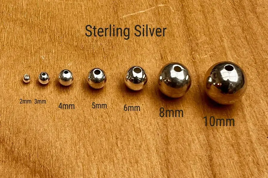
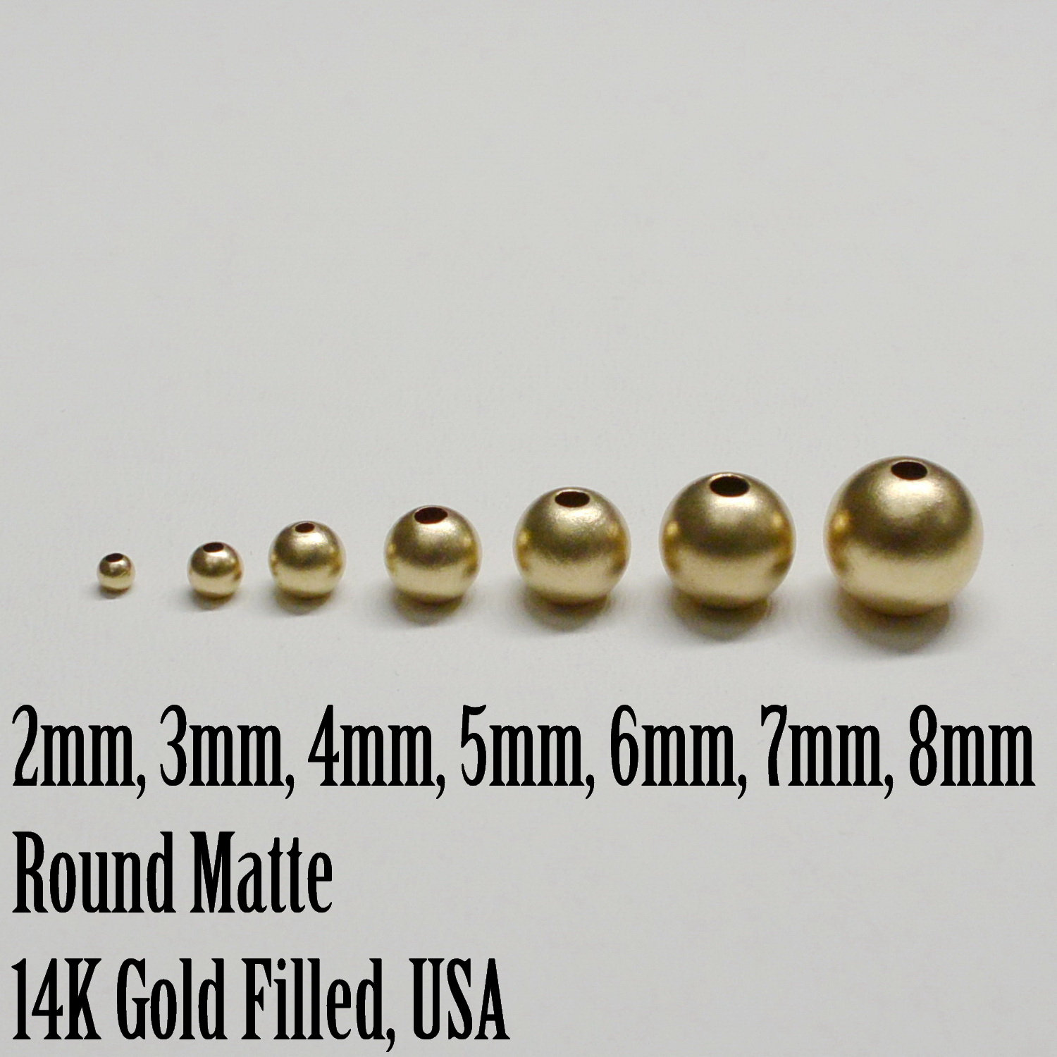
In an era defined by grand visions of artificial intelligence, expansive cloud infrastructures, and immersive virtual realities, it’s easy to overlook the microscopic details that form the bedrock of these monumental advancements. Yet, lurking within the specifications of nearly every device we interact with, from the smartphone in our pocket to the supercomputer powering complex simulations, are measurements so diminutive they seem inconsequential. One such measurement, 2 millimeters (mm), appears innocuous, an almost imperceptible gap or dimension. However, in the intricate world of technology, 2mm isn’t just a number; it’s a critical threshold, a boundary of precision, and often the difference between revolutionary functionality and frustrating failure.

To truly understand “what 2mm looks like” in technology, we must move beyond its literal interpretation as two small lines on a ruler. Instead, we must conceptualize it as a fundamental unit of engineering, design, and manufacturing prowess. It represents the relentless pursuit of miniaturization, the stringent demands of connectivity, and the delicate balance between form and function. This seemingly minor dimension underpins the performance, aesthetics, and even the very feasibility of the technological marvels we often take for granted. It’s in the unseen spaces, the tight tolerances, and the incredibly compact components where 2mm reveals its profound significance, shaping our digital lives in ways both subtle and substantial.
The Microcosm of Miniaturization: Where 2mm Reigns Supreme
The relentless drive towards smaller, more powerful, and energy-efficient devices has turned miniaturization into a foundational principle of modern technology. Within this microcosm, 2mm often signifies either a complete component or a critical feature whose scale dictates the overall design and performance of a system. The ability to pack more functionality into ever-decreasing volumes is a testament to human ingenuity and precise engineering, where 2mm can represent a significant chunk of real estate.
Silicon and Semiconductors: Beyond the Naked Eye
When we talk about the brains of modern electronics—microprocessors, memory chips, and graphic processing units—we are delving into a realm where dimensions are often measured in nanometers (billionths of a meter). However, the overall size of a chip package, or the spacing between critical elements on a circuit board, frequently involves millimeter-scale precision. A 2mm difference in chip package thickness, for instance, can dictate whether a smartphone remains sleek or becomes bulky. The physical dimensions of the die within the package, while much smaller, are encased in a housing that must be robust yet compact. Furthermore, the distance between connection pads (ball grid array – BGA or land grid array – LGA) on a chip can be on the order of 2mm, requiring incredible accuracy during the reflow soldering process to ensure perfect electrical contact across hundreds or even thousands of pins. The internal architecture of a System-on-Chip (SoC) might include various IP blocks, some of which, while performing complex functions, might occupy a physical area of just a few square millimeters, with individual components or interfaces within them being designed with 2mm constraints in mind.
Micro-Components and Sensors: Small but Mighty
Beyond the central processing units, countless other components operate at or around the 2mm mark, playing crucial roles in modern devices. Consider the passive components that filter signals and regulate power: surface-mount resistors and capacitors can easily be found in sizes like 0402 (0.04 x 0.02 inches, roughly 1mm x 0.5mm) or 0603 (1.6mm x 0.8mm). While smaller than 2mm individually, their collective arrangement and the necessary clearance around them contribute to the spatial economy where 2mm becomes a relevant benchmark.
More impressively, Micro-Electro-Mechanical Systems (MEMS) sensors—the accelerometers, gyroscopes, magnetometers, and barometers that give our devices an awareness of their physical orientation and environment—often have physical footprints of just a few square millimeters. A MEMS accelerometer, for example, might be encapsulated in a package that is 2mm x 2mm x 0.8mm. These tiny devices are marvels of engineering, integrating mechanical structures and electronic circuits on a single silicon chip to detect and convert physical phenomena into electrical signals. The intricate moving parts within them, though much smaller than 2mm, rely on the precise housing dimensions to function without interference. Similarly, miniature camera modules, especially those designed for endoscopes, drones, or wearable tech, push the boundaries of optics and sensor integration into incredibly compact form factors, often fitting within a 2mm cube or even smaller, demanding unparalleled manufacturing accuracy.
Connectivity and Fiber Optics: The Thread of Information
The digital age thrives on connectivity, and a significant portion of our global information infrastructure relies on fiber optics. Here, 2mm represents a critical dimension in several contexts. The core of a single-mode optical fiber, the actual conduit for light signals, is incredibly thin—typically 9 micrometers (0.009mm). However, this delicate core is protected by layers of cladding and buffering, bringing the total diameter of a single optical fiber strand to around 125 micrometers (0.125mm) or even 250 micrometers. When multiple such fibers are bundled into a cable for protection and ease of handling, the overall cable diameter can be a few millimeters. For instance, a common indoor fiber optic patch cable might have an outer diameter of 2mm or 3mm. This seemingly small diameter allows for an enormous capacity of data to be transmitted through a very compact medium, revolutionizing telecommunications and data centers. The precision required to cleave and splice these fibers, or to align them within a connector, ensures minimal signal loss, where a 2mm misalignment at critical junctions would render the connection useless.
Displaying Precision: 2mm in Visual Technology
The way we interact with technology is profoundly visual, making displays a central component of nearly every modern device. From the vastness of an LED billboard to the sharpness of a retina display, the quality of our visual experience is inextricably linked to precision, and here, 2mm can signify a pivotal dimension in both aesthetics and functionality.
Pixel Pitch and Resolution: The Canvas of Clarity
Pixel pitch refers to the distance between the centers of adjacent pixels on a display. This measurement is crucial for determining the optimal viewing distance and the perceived sharpness of an image. In large-format LED displays, such as those found in stadiums, concerts, or digital signage, pixel pitch can be several millimeters. For example, an outdoor LED screen might have a pixel pitch of P10 (10mm), meaning there are 10mm between the centers of each LED cluster. As displays become more refined, this pitch decreases. An indoor professional display might boast a P2.5 or P2 pixel pitch, meaning the distance between pixels is just 2.5mm or 2mm, respectively.
At a 2mm pixel pitch, individual pixels become virtually indistinguishable at a close viewing distance, delivering incredibly smooth images and text. This precision allows for stunning visual fidelity, making these displays ideal for command centers, broadcast studios, and high-end retail environments where detail is paramount. For smaller, personal screens like smartphones or tablets, the pixel pitch is far smaller than 2mm (often measured in hundreds of micrometers), but the concept of 2mm still highlights the continuous push for finer granularity, as current technologies strive for sub-millimeter pixel pitches to achieve “Retina” level clarity, where the human eye cannot discern individual pixels.
Bezels and Screen Thickness: The Edge of Immersion
The pursuit of an “all-screen” experience has driven manufacturers to relentlessly shrink the bezels—the borders around a display—to almost vanishing points. A 2mm bezel is considered ultra-thin, providing a near edge-to-edge viewing experience that maximizes screen real estate and enhances immersion. Achieving such slim bezels requires sophisticated engineering, including advanced display bonding techniques and intricate routing of display controller components. For laptops, monitors, and televisions, a 2mm bezel dramatically elevates the aesthetic appeal, making the content appear to float, uninterrupted, on the device.
Similarly, screen thickness is a critical metric for portability and sleek design. While the active display panel itself might be thin, the entire assembly, including the backlight unit (for LCDs), protective glass, and touch layers, contributes to the overall thickness. Reducing this total thickness to an astonishing 2mm (as seen in some ultra-thin OLED panels or concepts) is a significant engineering feat. It requires innovative material science for substrates and protective layers, as well as highly integrated control electronics, all meticulously designed to fit within this tight envelope without compromising structural integrity or display quality.
Projector Optics and Lasers: Focused Precision
In the realm of projection technology, 2mm signifies the kind of precision demanded by optical systems. The alignment of lenses, mirrors, and light sources within a projector, whether for home theater, business presentations, or industrial applications, is incredibly sensitive. A deviation of just 2mm in the focal length or alignment of an internal lens element could result in a blurry, distorted, or severely color-shifted image. High-end projectors, particularly those using laser light sources for enhanced brightness and color accuracy, require optical components to be manufactured and assembled with sub-millimeter tolerances to ensure perfect image geometry and uniform illumination. The actual diameter of some micro-lenses or the apertures through which laser beams pass can be designed with 2mm as a crucial reference point for their optical characteristics and interaction with other components. This level of exactitude is what allows for crisp, bright images projected across vast screens or even onto complex 3D surfaces.
The Tactile and Practical: 2mm in User Experience and Design
Beyond the purely technical, 2mm plays a profound role in how we physically interact with and perceive technology. It impacts ergonomics, the reliability of connections, and the very “feel” of our devices, demonstrating how a minute measurement can dictate comfort, convenience, and perceived quality.
Device Profiles and Ergonomics: The Hand-Held Difference
The physical dimensions of personal electronic devices are paramount to their ergonomics and portability. A 2mm difference in the thickness of a smartphone, tablet, or laptop can significantly alter how it feels in the hand or how easily it slips into a bag. Imagine a smartphone that is 10mm thick versus one that is 8mm. The 2mm reduction makes a tangible difference in perceived slenderness, comfort, and pocketability. Manufacturers invest heavily in shaving off these millimeters, often by integrating components more tightly, using thinner display technologies, or adopting advanced cooling solutions that take up less vertical space.
For wearables like smartwatches or fitness trackers, even a 2mm change in profile can dramatically affect comfort during prolonged wear. A device that feels too chunky or protrudes too much is less likely to be adopted or worn consistently. Industrial designers meticulously refine these dimensions, using 2mm as a common benchmark for making devices feel sleek, premium, and unobtrusive, striking a delicate balance between internal component requirements and external user experience.
Connectors and Ports: The Gateway to Functionality
Physical connectors and ports are the lifeblood of device interaction, enabling charging, data transfer, and peripheral connectivity. These components operate on extremely precise dimensions, where 2mm tolerances are fundamental to ensuring compatibility and reliable connections. Consider the ubiquitous USB-C port: its internal components and mating tolerances are designed with incredible precision. While the port itself is around 8.4mm wide and 2.6mm high, the internal contacts and their separation are measured in sub-millimeters, and the overall fit with a cable must be exact. A 2mm deviation in the manufacturing of either the port or the cable connector would prevent mating or lead to intermittent connectivity, causing immense frustration for users.
Similarly, the 3.5mm audio jack, though being phased out in many devices, is another prime example. Its 3.5mm diameter is a globally recognized standard. A 2mm error in this diameter, or in the length of the plug, would make it incompatible with the vast ecosystem of headphones and audio equipment. These standardized dimensions, often defined with millimeter-level precision, ensure universal interoperability, a crucial aspect of modern tech. Even proprietary connectors, like those found on certain smart devices or accessories, must adhere to strict 2mm or tighter tolerances to guarantee reliable mechanical and electrical coupling.
Haptic Feedback and Actuators: Subtle Vibrations, Big Impact
Haptic feedback systems, which provide tactile sensations through vibrations, are increasingly sophisticated, moving beyond simple buzzes to deliver nuanced “taps” and “clicks.” The actuators responsible for these sensations, such as linear resonant actuators (LRAs) or eccentric rotating mass (ERM) motors, are typically miniature components. An LRA, for example, might be a tiny, rectangular module measuring just 2mm x 4mm x 8mm. The precise movement of its internal mass, often a fraction of a millimeter in displacement, is carefully controlled to produce specific haptic effects.
The size and placement of these actuators within a device are critical. A 2mm reduction in their footprint allows designers to place them more strategically, closer to the user’s touch points, or to include multiple actuators for more localized and directional feedback. This miniaturization, with 2mm as a significant reference, enables the finely tuned haptic experiences that contribute to the premium feel and intuitive interaction of modern smartphones, game controllers, and smartwatches, transforming abstract digital inputs into tangible physical sensations.
Engineering Challenges and the Future of 2mm
The mastery of the 2mm dimension, and indeed, far smaller scales, is not achieved without overcoming significant engineering hurdles. Pushing the boundaries of miniaturization introduces a unique set of challenges related to manufacturing, materials science, and fundamental physics. Yet, these challenges also pave the way for future innovations, where today’s 2mm marvels inspire tomorrow’s even smaller wonders.
Manufacturing Precision and Tolerances: The Art of the Micro-Scale
Producing components and devices with 2mm (or smaller) critical dimensions demands unparalleled manufacturing precision. Traditional machining and assembly methods often fall short at these scales. Instead, advanced techniques like photolithography (for semiconductors), micro-injection molding, laser cutting, and additive manufacturing (3D printing) with incredibly fine resolution are employed. These processes operate with tolerances often in the micrometers (thousandths of a millimeter) to ensure that a 2mm part is exactly 2mm, not 2.01mm or 1.99mm.
The tools and machinery involved are themselves highly sophisticated, often operating in cleanroom environments to prevent even microscopic dust particles from interfering with production. Quality control at this scale also requires advanced metrology equipment, such as electron microscopes and atomic force microscopes, to verify dimensions and detect minute flaws. The cost and complexity associated with achieving and maintaining this level of precision are substantial, representing a significant portion of the research and development investment in the tech industry. The ability to consistently reproduce a 2mm feature with high yield is a hallmark of cutting-edge manufacturing.
Thermal Management at Micro-Scales: The Heat Problem
As components shrink to 2mm and below, and are packed more densely into devices, a critical challenge emerges: thermal management. Powering electronic circuits inevitably generates heat. At macroscopic scales, heat can dissipate through natural convection or larger heatsinks. However, within a 2mm space, or when multiple heat-generating components are within close proximity, heat becomes trapped. This can lead to overheating, reduced performance (thermal throttling), shortened component lifespan, and even device failure.
Engineers must devise ingenious solutions, such as ultra-thin vapor chambers, advanced thermal pastes with high conductivity, graphite sheets, or even liquid cooling systems miniaturized to fit within incredibly tight spaces. Designing materials that can efficiently conduct heat away from critical areas, while also maintaining structural integrity and electrical insulation, is an ongoing area of research. The 2mm constraint forces innovation in both materials science and thermal design, often requiring multi-disciplinary approaches to prevent devices from literally burning up under their own operational heat.
Emerging Tech: Nanobots and Bio-integration: Beyond 2mm
While 2mm represents a significant milestone in current miniaturization efforts, the horizon of technological advancement continually pushes towards even smaller scales. The mastery of manufacturing and integrating components at the millimeter and sub-millimeter level is a crucial stepping stone towards future technologies like nanobots and advanced bio-integrated electronics.
The precision engineering honed to produce 2mm components will be foundational for creating devices measured in micrometers and nanometers, destined for applications in medicine (e.g., targeted drug delivery, in-vivo diagnostics), advanced materials science, and environmental monitoring. Imagine microscopic robots, smaller than a grain of sand, navigating the human bloodstream, or bio-sensors seamlessly integrated with biological tissues. These futuristic visions, while currently operating at even finer scales, rely heavily on the foundational principles, materials, and manufacturing techniques perfected through the challenges of mastering the 2mm dimension. The journey to the nano-world begins with a firm grasp of the micro-world, where 2mm is a substantial boundary.
Conclusion
The question, “what does 2mm look like?” in the context of technology reveals far more than a simple linear measurement. It unveils a universe of precision engineering, design trade-offs, and relentless innovation. This seemingly insignificant dimension is a critical enabler across diverse technological domains, from the invisible circuits within a silicon chip to the tangible sleekness of a smartphone, the clarity of a display, and the reliability of a connector.
2mm represents the boundary where functionality meets form, where theoretical designs translate into practical, usable devices. It embodies the constant human drive to make technology more powerful, more accessible, and more integrated into our lives by making it smaller, lighter, and more efficient. The challenges associated with manufacturing, cooling, and designing within such tight tolerances push the limits of material science and engineering ingenuity, laying the groundwork for even more revolutionary advancements. As we continue to shrink the physical footprint of our digital world, the ability to command and conquer the 2mm space remains a testament to the profound impact of attention to detail and the quiet power of precision in shaping our technological future.
aViewFromTheCave is a participant in the Amazon Services LLC Associates Program, an affiliate advertising program designed to provide a means for sites to earn advertising fees by advertising and linking to Amazon.com. Amazon, the Amazon logo, AmazonSupply, and the AmazonSupply logo are trademarks of Amazon.com, Inc. or its affiliates. As an Amazon Associate we earn affiliate commissions from qualifying purchases.