
The Physics of Light and Digital Imaging Technology
In the rapidly advancing world of optical engineering and sensor technology, diffraction waves represent a fundamental phenomenon that dictates the theoretical limits of image clarity and resolution. While often discussed in abstract physics, diffraction is the defining constraint for the next generation of high-resolution image sensors, smartphone camera lenses, and advanced microscopy tools. Understanding how diffraction waves behave is essential for engineers and product developers working at the intersection of hardware optics and digital signal processing.
The Mechanism of Wave Propagation
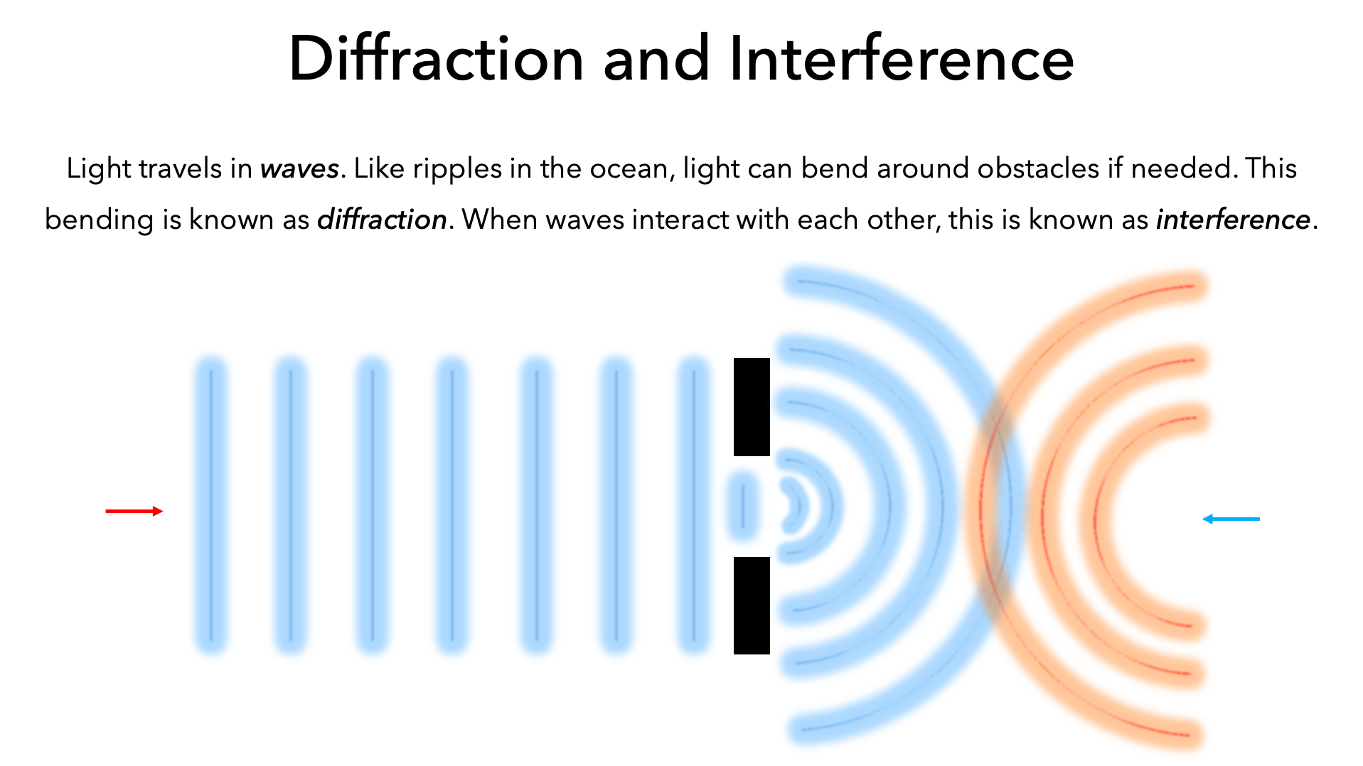
At its core, diffraction occurs when a wave—whether light, sound, or radio—encounters an obstacle or an aperture. Instead of traveling in a perfectly straight line, the wave bends around the edges of the obstacle, spreading out into the region beyond. In digital imaging, this happens every time light passes through a lens aperture. As light waves compress through a small opening, they interact with the edges of the lens housing or the aperture blades, resulting in a diffraction pattern known as the Airy disk.
For tech developers, this is not just a theoretical concern; it is the physical “speed limit” of optical performance. As pixels on modern CMOS sensors continue to shrink to capture more detail, they eventually reach a size where the diffraction-limited spot size is larger than the pixel itself. This leads to a loss of micro-contrast and resolution, forcing developers to rely on computational photography and AI-driven image restoration algorithms to mitigate the physical limitations of the lens.
Impact on Sensor Design and Pixel Pitch
The relationship between pixel pitch and diffraction is a critical metric in sensor hardware development. As manufacturers push for higher megapixel counts in smaller mobile devices, they often reduce the size of individual pixels. While smaller pixels theoretically offer higher resolution, they are significantly more sensitive to diffraction waves.
When the diameter of the Airy disk exceeds the pixel pitch, the optical signal essentially “blurs” across multiple pixels. This phenomenon is why increasing the megapixel count on a smartphone does not always result in a proportional increase in perceived sharpness. To combat this, hardware designers are increasingly utilizing backside-illuminated (BSI) sensors and stacked sensor architectures to maximize photon capture efficiency, effectively fighting the diffraction-limited degradation of the signal before it reaches the digital processing pipeline.
Computational Photography: Solving Physics with Software
Because diffraction waves impose a physical limit on what glass and silicon can achieve, the tech industry has pivoted toward computational photography to bridge the gap. When a camera can no longer capture a sharper image due to diffraction, the processing engine steps in to “deconvolve” the blur.
Deconvolution Algorithms
Deconvolution is a sophisticated mathematical process used to reverse the effects of diffraction. By modeling the Point Spread Function (PSF) of a lens—essentially a mathematical map of how that specific lens diffracts light—software engineers can apply an inverse filter to the raw data captured by the sensor. This technique effectively “resharpens” the image by predicting where the light waves were originally intended to land before they were spread out by the diffraction effect.
Modern smartphone SoCs (System-on-Chips) now dedicate specialized AI cores to these tasks. These processors run real-time restoration algorithms that analyze the metadata of the shot, identify the diffraction-induced blur, and selectively enhance edges and textures. This synergy between hardware limitations and software remediation is the primary driver of mobile photography innovation today.

Neural Networks and Sub-Pixel Restoration
The latest frontier in overcoming diffraction is the integration of deep learning. Unlike traditional deconvolution, which relies on rigid mathematical models, neural networks are trained on thousands of image pairs—some diffraction-limited and some captured under ideal conditions. Over time, these networks learn to hallucinate or reconstruct fine details that the sensor effectively lost to the diffraction wave.
This creates a new paradigm where “image quality” is no longer purely a product of optical glass quality, but rather the intelligence of the model processing the light signal. Tech companies are now effectively using AI to push past the Rayleigh Criterion—the classical physical limit of resolution—by inferring structural data that the optical system failed to resolve.
Future Trends: Beyond the Diffraction Limit
As we look toward the future of technology, the challenges posed by diffraction are spurring innovation in entirely new categories of hardware, specifically in metasurfaces and computational imaging.
Metasurfaces and Flat Optics
Traditional lenses rely on curvature to bend and focus light, which inherently creates the diffraction patterns we struggle with today. Metasurfaces, however, use nanostructured surfaces to manipulate light at the sub-wavelength level. By patterning the surface of a lens with millions of tiny, sub-micron “meta-atoms,” engineers can precisely control the phase of light waves.
This technology promises to replace bulky, diffraction-prone glass lenses with flat, wafer-thin surfaces that can correct for aberrations much more efficiently than traditional curved optics. By controlling light diffraction directly at the point of entry rather than attempting to clean it up after the fact, metasurfaces represent the next massive shift in optical hardware, potentially enabling everything from high-performance micro-drones to AR glasses with high-fidelity, thin-film optics.
Implications for Micro-Display and VR/AR
The impact of diffraction is not limited to photography. In the world of Extended Reality (XR) and VR headsets, diffraction is a significant hurdle. Many wave-guide displays used in augmented reality glasses rely on diffractive gratings to inject light into the eye. These systems must carefully manage diffraction to ensure that the image remains crisp and free of chromatic aberration.
Engineers in this sector are currently focused on “diffraction management”—designing gratings that steer light with surgical precision while minimizing the scattering that leads to “rainbow” artifacts or washed-out colors. As we move toward lighter, more portable AR devices, the ability to manipulate diffraction waves will determine which manufacturers can provide a truly immersive experience that feels indistinguishable from natural vision.

Balancing Physics and Digital Strategy
For companies operating in the hardware space, the strategy is clear: optics and processing are no longer two separate lanes. The most successful tech products are those that harmonize the physical hardware with the digital algorithms designed to handle the inevitable diffraction wave.
Investing in better glass remains vital, but it is only half the battle. The other half is ensuring that the digital signal processor (DSP) and the NPU (Neural Processing Unit) are tuned specifically to the diffraction profile of the lens optics. This holistic engineering approach—co-optimizing the physical lens design with the software-based restoration stack—defines the current state-of-the-art in digital imaging.
Ultimately, diffraction is a persistent physical constraint, but it is also a catalyst for innovation. By shifting our perspective from fighting diffraction as an enemy to engineering around it as a measurable constant, the tech industry continues to unlock higher levels of resolution, smaller form factors, and clearer visuals. Whether through the lens of a smartphone, a high-end microscope, or the next generation of AR eyewear, the mastery of the diffraction wave is what separates legacy hardware from the transformative technology of tomorrow.
aViewFromTheCave is a participant in the Amazon Services LLC Associates Program, an affiliate advertising program designed to provide a means for sites to earn advertising fees by advertising and linking to Amazon.com. Amazon, the Amazon logo, AmazonSupply, and the AmazonSupply logo are trademarks of Amazon.com, Inc. or its affiliates. As an Amazon Associate we earn affiliate commissions from qualifying purchases.