
NVIDIA, a name synonymous with high-performance graphics processing units (GPUs), has revolutionized industries from gaming and professional visualization to artificial intelligence and data centers. When users ask, “Where are NVIDIA GPUs made?”, the answer is far more intricate than pointing to a single factory or country. It’s a journey through a complex, globalized semiconductor supply chain, an elaborate dance of design innovation, cutting-edge fabrication, meticulous assembly, and sophisticated testing that spans continents. NVIDIA itself is a “fabless” company, meaning it designs its powerful chips but outsources the actual physical manufacturing to a network of highly specialized partners worldwide. Understanding this ecosystem is key to appreciating the marvel of modern technology production.
The Core of GPU Manufacturing: Fabrication Plants (Fabs)
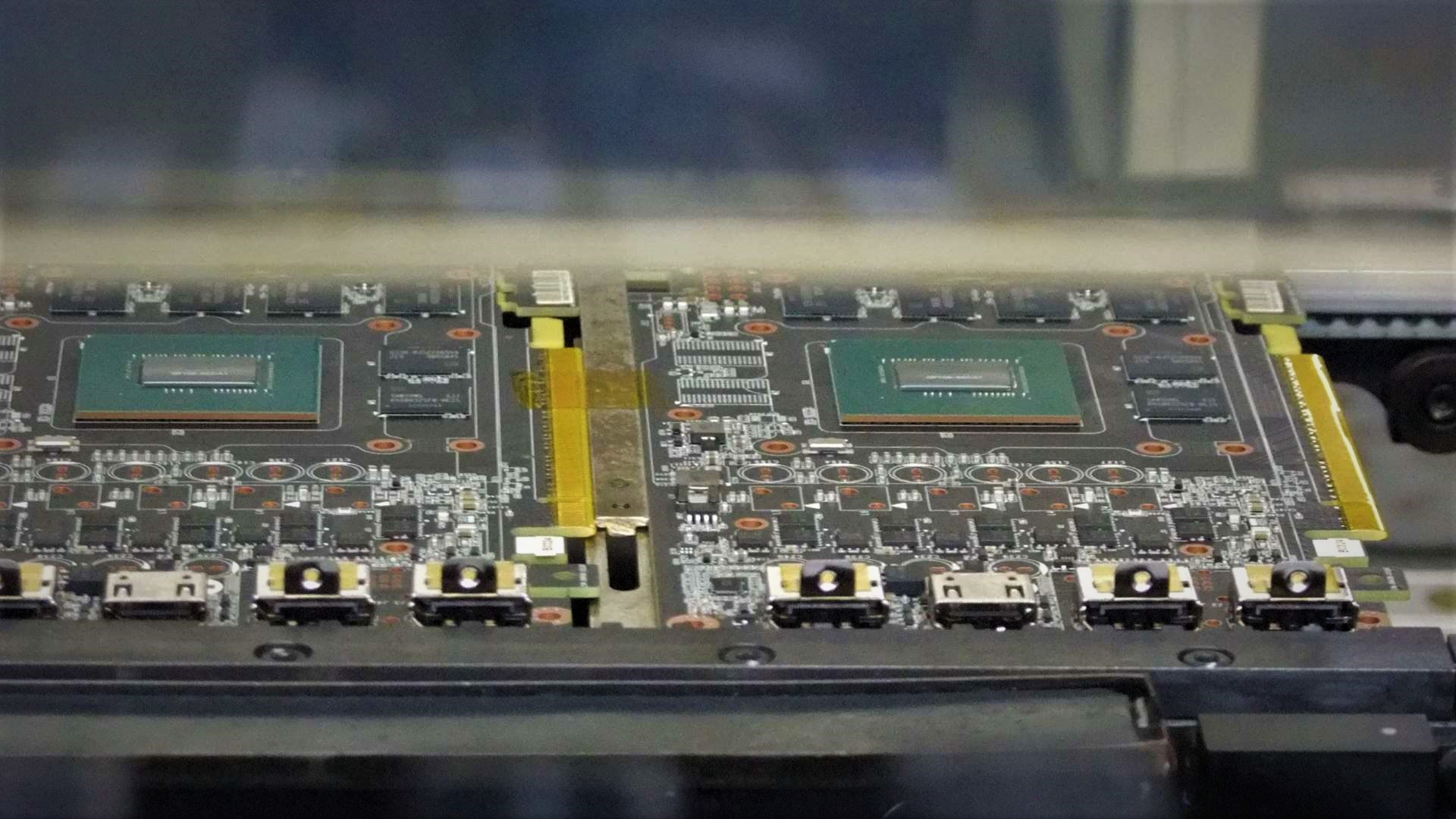
At the heart of a GPU’s birth is the fabrication plant, or “fab,” where silicon wafers are transformed into intricate integrated circuits. This is where the magic of semiconductor physics meets precision engineering on an atomic scale. For NVIDIA, this stage is predominantly handled by a select few leading foundries globally.
TSMC: NVIDIA’s Primary Foundry Partner
Taiwan Semiconductor Manufacturing Company (TSMC) stands as NVIDIA’s primary and most crucial fabrication partner, especially for its most advanced and powerful GPUs. TSMC is the world’s largest dedicated independent semiconductor foundry, a true titan in the industry. Based primarily in Hsinchu, Taiwan, TSMC operates a vast network of advanced fabs, including several “gigafabs” capable of producing millions of wafers annually.
NVIDIA relies on TSMC for its cutting-edge process nodes, such as 5nm, 4nm, and the upcoming 3nm technologies. These nanometer figures refer to the transistor gate length, indicating the density and performance capabilities of the chips. The smaller the number, the more transistors can be packed onto a single die, leading to greater computational power and energy efficiency—critical factors for NVIDIA’s demanding GPUs used in AI, high-end gaming, and professional applications. TSMC’s unparalleled expertise, massive production capacity, and consistent innovation in process technology make it an indispensable partner for NVIDIA. While the majority of these advanced fabrication facilities are located in Taiwan, TSMC is also expanding its global footprint with new fabs under construction or planned in Arizona (USA), Japan, and potentially Germany, driven by geopolitical considerations and the desire for supply chain diversification.
Samsung Foundry: A Strategic Alternative
While TSMC handles the bulk of NVIDIA’s leading-edge production, Samsung Foundry serves as another critical, albeit often secondary, fabrication partner. Samsung, a South Korean conglomerate, possesses its own world-class semiconductor manufacturing capabilities. NVIDIA has leveraged Samsung Foundry for specific product lines or generations, sometimes to diversify its supply chain, mitigate risks, or capitalize on competitive pricing and technological offerings. For instance, some of NVIDIA’s previous-generation consumer GPUs utilized Samsung’s 8nm or 7nm process nodes.
Working with multiple foundries provides NVIDIA with strategic flexibility. It fosters healthy competition between the manufacturers, potentially leading to better terms and accelerated technological advancements. It also provides a crucial layer of redundancy, ensuring that potential disruptions at one foundry do not cripple NVIDIA’s entire production pipeline.
The “Fabless” Model Explained
NVIDIA operates on a “fabless” business model, a strategic decision that has become common among many leading semiconductor companies. In this model, NVIDIA focuses intensely on its core competencies: research and development (R&D), chip architecture design, intellectual property creation, and marketing. They design the intricate layouts of their GPUs down to the individual transistor, develop the software and drivers, and manage the product roadmap.
By outsourcing the capital-intensive and highly specialized manufacturing processes to foundries like TSMC and Samsung, NVIDIA avoids the monumental costs associated with building and maintaining cutting-edge fabrication plants, which can run into tens of billions of dollars per facility. This model allows NVIDIA to allocate its resources primarily towards innovation, pushing the boundaries of GPU technology without the burden of manufacturing infrastructure, giving them agility and focus in a rapidly evolving market.
Beyond the Wafer: Assembly, Testing, and Packaging (ATP)
Once the silicon wafers leave the fabrication plant, the journey of an NVIDIA GPU is far from over. The raw wafers contain hundreds, sometimes thousands, of individual GPU “dies” (the actual silicon chips). These dies must be separated, packaged, and thoroughly tested before they can be integrated into a functional graphics card or other computing device. This crucial stage is known as Assembly, Testing, and Packaging (ATP).
The Intricacies of ATP
The ATP process is a highly sophisticated series of steps designed to transform raw silicon dies into robust, functional, and reliable components. It begins with “wafer dicing,” where the wafer is cut into individual dies. Each die then undergoes initial testing to identify and discard defective units. The good dies are then carefully attached to a substrate, a small circuit board that provides electrical connections and mechanical support.
Following this, the die is “packaged.” Modern GPUs utilize advanced packaging technologies like flip-chip ball grid array (FCBGA), where the die is inverted and connected directly to the substrate via an array of tiny solder balls. This allows for high-density interconnections and improved electrical performance. A heat spreader is then typically attached to the top of the package, often with a thermal interface material (TIM) in between, to aid in heat dissipation. The final step involves comprehensive functional testing, where each packaged GPU is subjected to rigorous tests to ensure it meets NVIDIA’s stringent performance, power, and reliability specifications. This includes running diagnostic programs, stressing the chip, and checking for any defects or anomalies.
Global ATP Hubs
The ATP stage is typically carried out in specialized facilities located in various global hubs, predominantly in Southeast Asia and East Asia. Countries like Malaysia, Vietnam, the Philippines, China, and Taiwan are renowned for their advanced ATP capabilities. These regions offer a combination of skilled labor, sophisticated infrastructure, and established supply chain networks that are vital for high-volume semiconductor production.
Companies such as ASE Technology Holding (Advanced Semiconductor Engineering), Amkor Technology, and Siliconware Precision Industries (SPIL) are prominent players in the Outsourced Semiconductor Assembly and Test (OSAT) industry, often partnering with NVIDIA and other fabless companies to handle this complex post-fabrication work. Their facilities are equipped with highly automated machinery and specialized cleanrooms to ensure precision and prevent contamination.
NVIDIA’s Role in Quality Assurance
Despite outsourcing the ATP process, NVIDIA maintains a vigilant role in quality assurance and control. NVIDIA’s engineers work closely with their OSAT partners to define testing methodologies, performance benchmarks, and quality standards. They provide detailed specifications for packaging, thermal performance, and reliability.
NVIDIA also deploys its own teams to audit and oversee the production lines at partner facilities, ensuring that protocols are strictly followed and that the final products meet the exact specifications of their designs. This continuous oversight is crucial for guaranteeing the integrity and performance of every NVIDIA GPU that reaches the market, maintaining the brand’s reputation for cutting-edge and reliable hardware.
The Broader Ecosystem: Components and Design
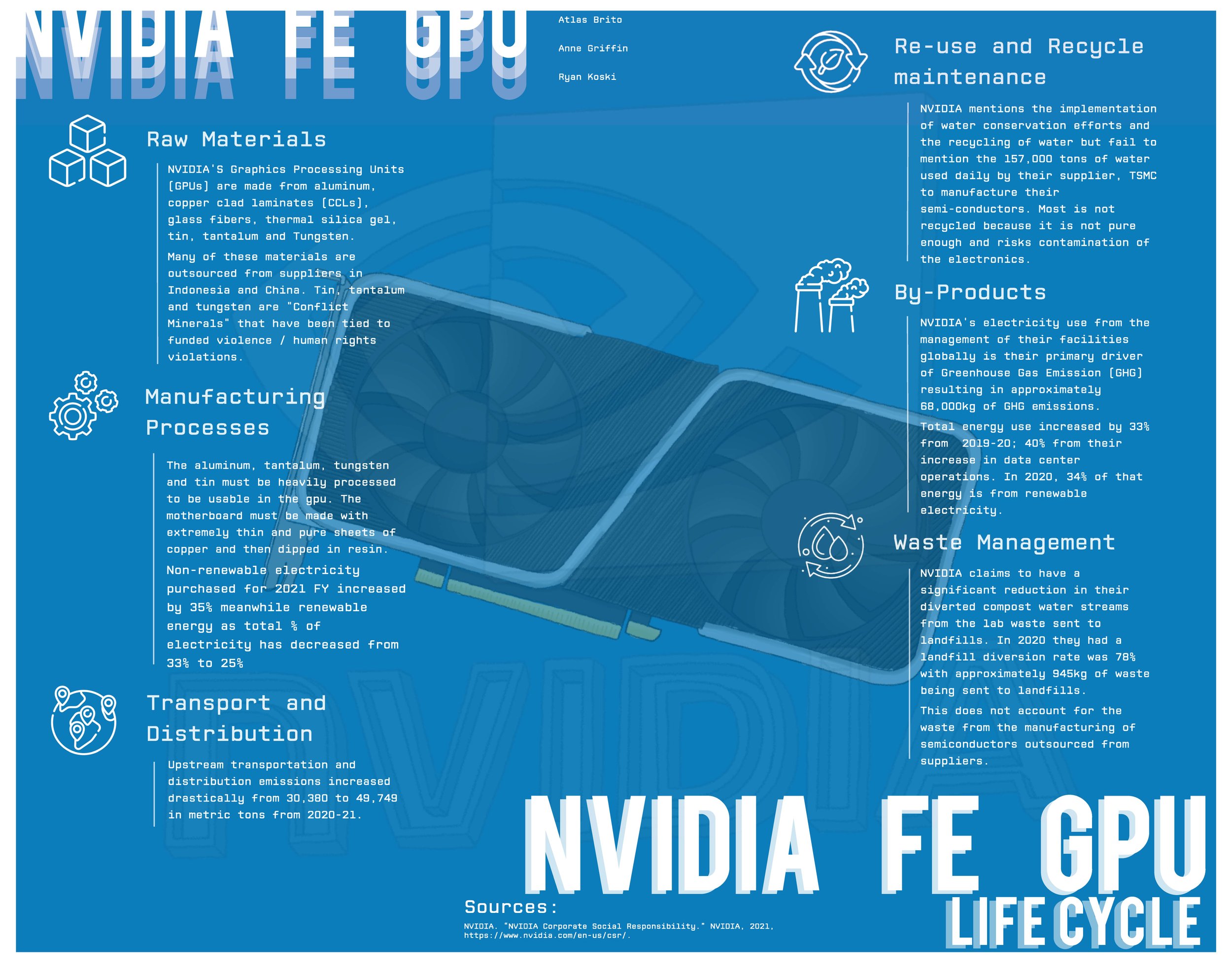
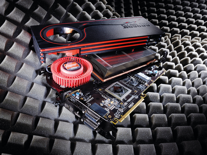
A complete NVIDIA GPU, as found on a graphics card, is much more than just the central processing unit. It’s an intricate amalgamation of various components, each manufactured by specialized suppliers across the globe, all orchestrated by NVIDIA’s overarching design.
Memory Modules (GDDR, HBM)
Modern GPUs demand incredibly fast memory to feed their immense processing power. NVIDIA GPUs primarily utilize GDDR (Graphics Double Data Rate) memory, with the latest generations employing GDDR6 or GDDR6X, and some high-performance computing (HPC) and data center GPUs featuring HBM (High Bandwidth Memory). These memory chips are typically manufactured by leading memory producers such as Samsung, SK Hynix (South Korea), and Micron Technology (USA). These companies have their own sophisticated fabrication and packaging facilities, often located in their respective home countries or other East Asian manufacturing hubs. These memory modules are then integrated onto the GPU package or the graphics card’s PCB alongside the main GPU die.
Printed Circuit Boards (PCBs)
The GPU chip, along with its memory modules and other discrete components, is mounted onto a Printed Circuit Board (PCB). The PCB serves as the physical foundation, providing the electrical pathways (traces) that connect all the components and the necessary power delivery network. PCBs for NVIDIA graphics cards are manufactured by specialized PCB fabrication houses, predominantly located in China, Taiwan, and other parts of Asia. These manufacturers create multi-layered boards with extreme precision to handle the high-speed signals and power requirements of modern GPUs.
Cooling Solutions and Other Components
Beyond the core silicon, a functioning graphics card requires a sophisticated cooling solution, power delivery components, and various connectors. Heatsinks, often made of copper and aluminum, and fan assemblies are designed to dissipate the significant heat generated by high-performance GPUs. These components are typically produced by specialized manufacturers in Asia, often in China, which has a vast ecosystem for electronics manufacturing. Capacitors, resistors, voltage regulators, and other discrete electronic components are sourced from a global network of suppliers. Even the external ports (HDMI, DisplayPort) and power connectors have their own distinct supply chains.
NVIDIA’s Design and R&D Centers
Crucially, while the physical manufacturing is distributed, the intellectual genesis of NVIDIA GPUs resides firmly within NVIDIA itself. NVIDIA’s research and development centers, notably headquartered in Santa Clara, California, and with significant engineering hubs across the globe (e.g., Austin, Bangalore, Shanghai, Helsinki), are where the magic truly begins. This is where brilliant engineers and scientists conceive new architectures, design intricate circuits, develop advanced algorithms, and create the foundational technologies (like CUDA) that make NVIDIA GPUs so powerful. These centers are the birthplace of the Hopper, Ada Lovelace, Ampere, and Pascal architectures, ensuring that the “brain” of the GPU is entirely NVIDIA’s creation, guiding the global manufacturing process.
Supply Chain Dynamics and Geopolitical Implications
The global semiconductor supply chain, as exemplified by NVIDIA’s GPU production, is a marvel of efficiency and specialization, but it is also inherently vulnerable to disruptions and influenced by geopolitical forces.
Resiliency and Diversification
The industry is constantly striving for greater resiliency. Lessons learned from natural disasters, trade disputes, and most recently, the COVID-19 pandemic, have highlighted the fragility of highly concentrated supply chains. This has led companies like NVIDIA and their partners to actively seek diversification, distributing production across different regions and even exploring new partners to mitigate the risk of single points of failure. The goal is to build a more robust and adaptable supply network that can withstand unforeseen challenges.
Government Incentives and Localization
Governments worldwide recognize the strategic importance of semiconductor manufacturing, given its foundational role in almost every aspect of modern technology and national security. Countries like the United States (via the CHIPS Act), the European Union (EU Chips Act), Japan, and others are investing massive sums to incentivize semiconductor companies to build new fabrication and ATP facilities within their borders or diversify existing ones. The aim is to reduce reliance on specific regions, particularly Taiwan, which currently dominates advanced chip manufacturing, and to create more localized or regionally balanced supply chains. These initiatives are leading to the construction of new fabs in places like Arizona and Germany, which will eventually contribute to the global production capacity for chips, including potentially those destined for NVIDIA.
The Impact of Global Events
Global events can send ripples throughout this interconnected supply chain. The pandemic exposed vulnerabilities, leading to widespread chip shortages that impacted numerous industries, including automotive, consumer electronics, and even certain segments of the GPU market. Geopolitical tensions, such as those between the U.S. and China or concerns around cross-strait relations involving Taiwan, can also profoundly influence investment decisions, trade policies, and the overall stability of the semiconductor industry. NVIDIA, as a key player, continuously navigates these complex dynamics, adapting its strategies to ensure a consistent and reliable supply of its products.
Conclusion
Asking “where are NVIDIA GPUs made?” unveils a story of remarkable global collaboration and technological prowess. It’s not a single factory, but a sophisticated, multi-stage process involving specialized partners across continents. From the highly advanced foundries in Taiwan and Korea that fabricate the silicon wafers, to the assembly, testing, and packaging facilities in Southeast Asia, and the countless suppliers of memory, PCBs, and cooling solutions, NVIDIA’s GPUs are a product of a vast, interconnected ecosystem. While the physical manufacturing is outsourced, the core innovation, design, and quality oversight remain firmly rooted within NVIDIA’s R&D centers globally. This intricate supply chain not only drives NVIDIA’s success but also underscores the interdependent nature of modern technology, continuously adapting to innovation, market demands, and evolving geopolitical landscapes to power the future of computing.
aViewFromTheCave is a participant in the Amazon Services LLC Associates Program, an affiliate advertising program designed to provide a means for sites to earn advertising fees by advertising and linking to Amazon.com. Amazon, the Amazon logo, AmazonSupply, and the AmazonSupply logo are trademarks of Amazon.com, Inc. or its affiliates. As an Amazon Associate we earn affiliate commissions from qualifying purchases.