
In the rapidly evolving landscape of nanotechnology, semiconductor manufacturing, and materials science, the ability to analyze the surface of a material at the atomic level is not just an advantage—it is a necessity. Among the most powerful tools in the modern technologist’s arsenal is Auger Electron Spectroscopy (AES). As industries push toward smaller, faster, and more efficient components, understanding the chemical composition of the topmost layers of a material has become a critical pillar of research and development. This article explores the mechanics, instrumentation, and industrial applications of AES, positioning it as a cornerstone of high-tech analytical methodology.
The Physics Behind the Beam: How Auger Electron Spectroscopy Works
At its core, Auger Electron Spectroscopy is a surface-sensitive analytical technique used specifically to determine the elemental composition and, in some cases, the chemical state of the surfaces of solids. The technique is named after Pierre Victor Auger, a French physicist who independently discovered the process in the 1920s. To understand how AES works, one must dive into the quantum interactions between electrons and atoms.
The Core Principles: Electron Bombardment
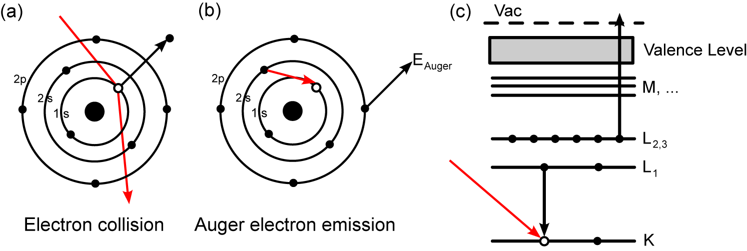
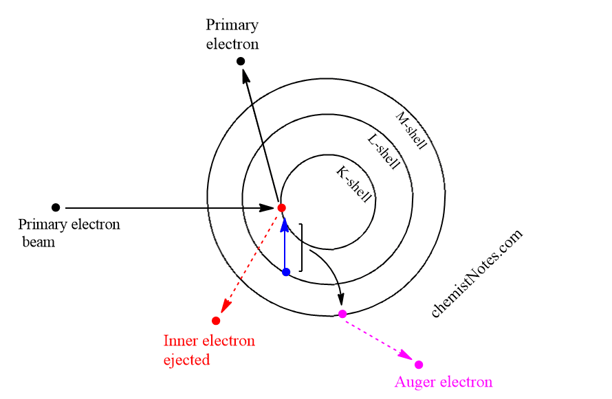
The process begins with an external source of energy, typically a focused beam of primary electrons with energies ranging from 2 to 10 keV. When this primary beam strikes the surface of a sample, it interacts with the atoms in the material. If a primary electron has sufficient energy, it can kick out a core-level electron from an atom, creating a “hole” or a vacancy in an inner shell (such as the K-shell). This leaves the atom in an unstable, highly excited state.
The Relaxation Process: The Auger Effect
To regain stability, an electron from a higher energy level (an outer shell) drops down to fill the vacancy created by the primary beam. This transition releases energy. In some instances, this energy is emitted as a photon (X-ray fluorescence). However, in the Auger process, the energy released is transferred to a third electron, typically from an outer shell. This third electron—the Auger electron—is then ejected from the atom.
The crucial characteristic of the Auger electron is its kinetic energy. Because the energy levels of every element are unique and quantized, the kinetic energy of the ejected Auger electron is a “fingerprint” of the element from which it originated. By measuring these energies, scientists can identify exactly which elements are present on the surface of the sample.
Energy Mapping and Chemical Fingerprinting
Because Auger electrons have relatively low kinetic energies (typically between 50 eV and 3,000 eV), they cannot travel far through a solid without losing energy due to collisions. Consequently, only those Auger electrons generated within the first 1 to 5 nanometers of the surface can escape the material and reach the detector. This inherent limitation is what makes AES a “surface-sensitive” technique, providing high-resolution data that bulk analysis methods simply cannot match.
Hardware and Instrumentation: The Tools of the Trade
Performing Auger Electron Spectroscopy requires a sophisticated suite of hardware designed to operate under extreme conditions. The “tech” behind the machine is as impressive as the physics it measures, involving precision vacuum systems, electron optics, and advanced signal processing.
The Ultra-High Vacuum (UHV) Environment
One of the most critical components of an AES system is the vacuum chamber. AES must be performed under Ultra-High Vacuum (UHV) conditions, typically reaching pressures lower than $10^{-9}$ torr. There are two primary reasons for this. First, a vacuum is necessary to allow the electron beam and the emitted Auger electrons to travel to and from the sample without colliding with gas molecules. Second, because AES is so sensitive to the surface, even a single layer of gas molecules adsorbed from the atmosphere would obscure the sample and provide false readings. Maintaining a UHV environment ensures that the surface remains clean for the duration of the analysis.
Electron Guns and Analyzers
The “eyes” of the AES system consist of the electron gun and the energy analyzer. Modern AES systems use Field Emission (FE) electron guns, which can produce incredibly narrow beams (down to 10 nanometers or less). This allow for “Auger Mapping,” where the beam scans across the surface to create a two-dimensional map of elemental distribution.
Once the Auger electrons are ejected, they are captured by an analyzer, most commonly a Cylindrical Mirror Analyzer (CMA) or a Hemispherical Sector Analyzer (HSA). These components use electric fields to filter electrons based on their kinetic energy, allowing only those with specific energies to reach the detector at any given time.
Data Processing and Imaging Software
The raw data collected by the detector is a complex spectrum of electron counts versus energy. Modern AES software employs sophisticated algorithms to differentiate the relatively small Auger peaks from the high background noise caused by secondary and backscattered electrons. This software often allows for “Depth Profiling,” where an ion gun is used to etch away layers of the sample surface atom-by-atom, allowing the AES system to analyze the composition of the material as it moves deeper into the structure.
Real-World Applications in High-Tech Industries
AES is not merely a theoretical tool; it is a workhorse in industries where surface chemistry dictates performance. From the smartphone in your pocket to the satellites orbiting the Earth, AES has likely played a role in their development.
Semiconductor Fabrication and Failure Analysis
In the semiconductor industry, “smaller” is always the goal. As transistors shrink to the 5nm or 3nm scale, even a trace amount of contamination can lead to catastrophic failure. AES is used to verify the purity of thin films and to analyze the interfaces between different layers of a microchip. If a batch of chips fails, engineers use AES to perform failure analysis, identifying whether an unwanted element (like oxygen or carbon) has leaked into a critical junction.
Nanotechnology and Surface Chemistry
The field of nanotechnology relies heavily on the surface-to-volume ratio. Because nanomaterials have so much surface area relative to their mass, their surface properties dominate their behavior. AES allows nanotechnologists to characterize nanoparticles, nanotubes, and graphene layers with unprecedented precision. It is used to study how catalysts react at the surface level, which is essential for developing new energy solutions like hydrogen fuel cells and high-capacity batteries.
Corrosion and Metallurgical Research
For the aerospace and automotive industries, understanding how metals interact with their environment is vital for safety and longevity. AES is used to study the early stages of corrosion and the formation of oxide layers. By analyzing the “passivation layer” (the protective film that forms on metals like aluminum or stainless steel), tech companies can develop new alloys and coatings that are more resistant to extreme environments.
AES vs. Other Analytical Techniques: A Tech Comparison
When a lab needs to analyze a surface, they often choose between AES and several other technologies. Understanding why a technician would choose AES over another method is key to understanding its niche in the tech world.
AES vs. XPS (X-ray Photoelectron Spectroscopy)
XPS is the primary competitor to AES. While both are surface-sensitive, they use different excitation sources; XPS uses X-rays, while AES uses an electron beam. The primary advantage of AES is its spatial resolution. Because electron beams can be focused much more tightly than X-ray beams, AES can analyze features as small as 10nm, whereas standard XPS is typically limited to tens of micrometers. However, XPS is generally better at providing detailed “chemical state” information (e.g., distinguishing between different types of carbon-oxygen bonds).
AES vs. SEM (Scanning Electron Microscopy)
Many AES systems are actually built into or alongside Scanning Electron Microscopes. While SEM provides incredible topographical images (the “look” of the surface), it does not inherently provide chemical information. By adding an Auger detector to an SEM setup, a researcher can see a high-resolution image of a defect and then immediately perform a chemical analysis on that exact spot to see what it is made of.
Future Trends: The Evolution of Auger Technology
As we look toward the future, Auger Electron Spectroscopy continues to evolve, driven by the demands of the next generation of technology.
Enhancing Spatial Resolution with AI
One of the most exciting trends in AES is the integration of Artificial Intelligence and Machine Learning in data interpretation. AI algorithms can now assist in deconvolution—separating overlapping energy peaks that were previously indistinguishable. This allows for even higher sensitivity, enabling the detection of trace elements at levels that were once considered “noise.”
Integration with Multi-Technique Platforms
The future of materials analysis lies in “cluster tools”—vacuum systems that house multiple analytical techniques (AES, XPS, SIMS, and SEM) in a single ultra-high vacuum environment. This allows a sample to be analyzed by four or five different technologies without ever being exposed to air. This holistic approach is becoming the standard for developing quantum computing components and next-generation photovoltaic cells.

Conclusion
Auger Electron Spectroscopy remains an indispensable pillar of modern technology. By leveraging the unique quantum interactions of the Auger effect, it provides a window into the atomic world that few other techniques can offer. Whether it is ensuring the reliability of a microprocessor, pioneering new nanomaterials, or preventing the corrosion of aerospace alloys, AES provides the data-driven insights that fuel innovation. As our technological ambitions move deeper into the nanoscale, the precision and surface sensitivity of AES will continue to be a primary driver of scientific and industrial progress.
aViewFromTheCave is a participant in the Amazon Services LLC Associates Program, an affiliate advertising program designed to provide a means for sites to earn advertising fees by advertising and linking to Amazon.com. Amazon, the Amazon logo, AmazonSupply, and the AmazonSupply logo are trademarks of Amazon.com, Inc. or its affiliates. As an Amazon Associate we earn affiliate commissions from qualifying purchases.