
In the rapidly evolving landscape of semiconductor technology, we often focus on the nanometer scale of transistors or the architectural brilliance of new GPUs. However, there is a silent hero in the world of high-performance computing that remains largely invisible to the average consumer: ABF.
ABF stands for Ajinomoto Build-up Film. While the name might sound more at home in a culinary laboratory than a high-tech cleanroom, ABF is perhaps the most critical material in modern chip packaging. Without it, the powerful processors driving artificial intelligence, 5G networks, and autonomous vehicles simply would not function. This article explores the technical nuances of ABF, its historical origins, and why it has become the ultimate bottleneck in the global tech supply chain.

The Science Behind ABF Substrate
To understand ABF, one must first understand the “package.” A semiconductor chip (the die) is incredibly fragile and uses microscopic connections. It cannot be soldered directly onto a standard printed circuit board (PCB). Instead, it sits on a “substrate”—a specialized interlayer that translates the tiny connections of the chip into the larger connections of the motherboard. ABF is the material used to create these complex, multi-layered substrates.
From MSG to Microchips: The Surprising History
The story of ABF is one of the most fascinating pivots in industrial history. It was developed by the Ajinomoto Group, a Japanese company primarily known for producing monosodium glutamate (MSG) and other food products. In the 1970s, the company began exploring the chemistry of epoxy resins, a byproduct of their amino acid fermentation processes.
By the late 1990s, as CPUs became more powerful, the industry moved away from “lead frame” packaging toward “build-up” substrates. Traditional liquid insulators were difficult to apply evenly and slowed down production. Ajinomoto’s researchers realized that an insulating film—rather than a liquid—could solve these problems. In 1999, the first ABF-based CPUs hit the market, and today, it is the industry standard for nearly all high-end logic chips.
Technical Composition and Insulation Properties
ABF is a thermosetting film composed of epoxy resin, hardeners, and inorganic fillers. Its primary function is to serve as an electrical insulator between the multiple layers of circuitry within a chip substrate.
What makes ABF unique is its “smoothness” and receptivity to laser processing. As transistors shrunk, the wiring on the substrate had to become denser. ABF allows for the drilling of microscopic holes, known as “vias,” using lasers. These vias connect different layers of the substrate with incredible precision, ensuring that signals can travel at high speeds without interference or data loss.
The Build-Up Process in Circuitry
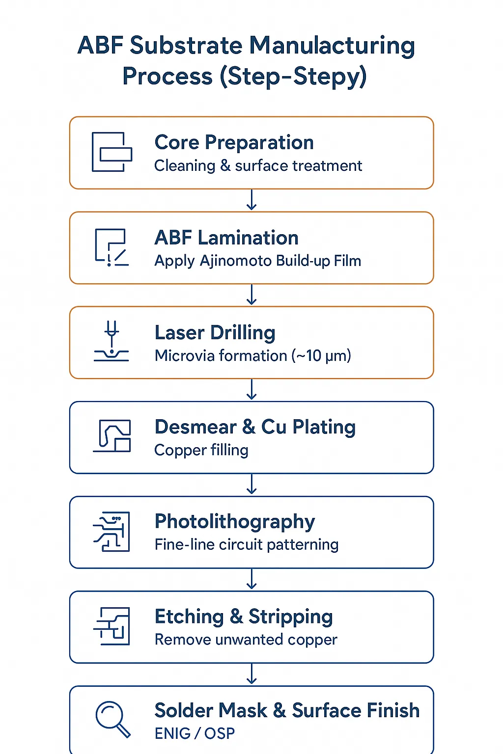
The term “Build-up” in ABF refers to the manufacturing methodology. Instead of creating a single thick board, manufacturers build the substrate layer by layer. A layer of ABF is laminated onto a core, holes are drilled, circuit patterns are plated with copper, and then another layer of ABF is applied. This “stacking” allows for high-density interconnect (HDI) designs that are essential for the massive pin counts found on modern processors like NVIDIA’s H100 or Intel’s Xeon Scalable processors.
Why ABF is the Backbone of the AI Revolution
The current explosion in Artificial Intelligence (AI) and Machine Learning (ML) has placed ABF in the spotlight. AI models require massive amounts of data throughput, which translates to a need for larger, more complex chip packages.
Powering High-Performance Computing (HPC)
High-Performance Computing (HPC) relies on “chiplets”—a design philosophy where several smaller chips are combined into one large package. To facilitate communication between these chiplets, the substrate must be extremely large and feature dozens of layers. ABF is the only material that currently meets the thermal stability and insulation requirements for these massive HPC packages. As AI companies demand more powerful chips, the surface area of ABF used per chip has increased exponentially.
The Role in GPU and CPU Packaging
Whether it is the latest gaming GPU or a server-side CPU, ABF is the connective tissue. In the consumer space, the push for 4K gaming and real-time ray tracing requires GPUs to handle immense electrical loads. ABF’s ability to resist heat deformation ensures that these chips remain stable even under heavy overclocking. In the enterprise sector, the reliability of ABF-based substrates is a prerequisite for the “five nines” (99.999%) of uptime required by data centers.
Enabling 5G and Autonomous Driving
Beyond the data center, ABF is critical for the infrastructure of the future. 5G base stations require high-frequency signal processing, which is highly sensitive to the dielectric properties of the substrate. ABF provides the low-loss environment necessary for millimeter-wave technology. Similarly, in autonomous vehicles, the “brain” of the car (the ADAS system) requires heavy-duty processing power packaged in a way that can survive the vibrations and temperature fluctuations of a moving vehicle—parameters that ABF-based substrates are designed to handle.
The Global Supply Chain and the ABF Shortage
Despite its importance, the production of ABF is a significant bottleneck. This has led to widespread industry concern regarding “substrate shortages,” which often delay the release of new technology more than the actual silicon fabrication.
Why Production Capacity is a Bottleneck
The production of ABF-based substrates is an incredibly capital-intensive and low-yield process. Unlike the silicon chips themselves, which can be produced in massive quantities via photolithography, the “build-up” process for substrates is mechanical and chemical.
Furthermore, the Ajinomoto Group remains the sole provider of the high-quality film required for high-end chips. While there are other film manufacturers, the “Ajinomoto” brand of film is the only one qualified by major giants like Intel, AMD, and NVIDIA for their flagship products. This “single-point-of-failure” in the supply chain means that any disruption at Ajinomoto or the primary substrate manufacturers can halt global tech production.
Key Players in the ABF Ecosystem
The ABF ecosystem is divided into the film producer (Ajinomoto) and the substrate manufacturers (the companies that buy the film to build the boards). Key players include:
- Unimicron (Taiwan): One of the largest substrate makers in the world, heavily invested in by Intel.
- Ibiden (Japan): A pioneer in high-end substrate technology.
- Nan Ya PCB (Taiwan): A major supplier for both consumer and industrial electronics.
- Samsung Electro-Mechanics (South Korea): Recently expanding into the high-end server substrate market.
Future Projections and Market Stability
To mitigate shortages, these manufacturers have invested billions of dollars in new factories. However, a new substrate plant takes 2–3 years to reach full production capacity. As we move into 2025 and beyond, the market is expected to stabilize, but the demand for “large-area” substrates (used in AI) continues to outpace the growth of the manufacturing lines. This means that while standard ABF substrates may become cheaper, the “bleeding-edge” substrates will remain a premium, scarce commodity.
Innovations and Alternatives in Semiconductor Packaging
As we approach the physical limits of organic materials like ABF, the tech industry is already looking toward the next frontier of packaging.
Beyond Organic Substrates: Glass and Silicon Interposers
While ABF is an “organic” substrate (based on epoxy resins), there is a growing movement toward inorganic materials. Glass substrates are currently being researched by companies like Intel as a potential successor to ABF. Glass offers superior flatness and thermal stability, which allows for even denser wiring. However, glass is brittle and difficult to manufacture at scale.
Another alternative is the Silicon Interposer (used in TSMC’s CoWoS technology). This uses a thin sliver of silicon to connect chips. While faster than ABF, silicon interposers are significantly more expensive and are currently reserved only for the most elite AI chips, such as the NVIDIA H200.
The Environmental Impact of Semiconductor Materials
In an era where “Green Tech” is a priority, the chemical nature of ABF is under scrutiny. The production of epoxy resins involves complex chemical syntheses. The industry is currently exploring bio-based resins and more efficient recycling methods for discarded PCBs and substrates. As the volume of ABF production increases to meet AI demands, the pressure on the Ajinomoto Group and its partners to innovate sustainable manufacturing processes will likely become a primary focus of their R&D departments.
Conclusion
ABF is a testament to the fact that the most advanced technology in the world often relies on fundamental material science. From its humble origins in food chemistry to its current status as the gatekeeper of the AI revolution, Ajinomoto Build-up Film has redefined how we build computers.
As we look forward, the role of ABF will only expand. Whether it is through the continued refinement of organic films or the eventual transition to glass-based systems, the “substrate” will remain the foundation of the digital world. Understanding ABF is not just about understanding a piece of plastic; it is about understanding the structural requirements of the intelligence age. For the tech industry, the lesson is clear: no matter how fast your processor is, it is only as good as the film that holds it together.
aViewFromTheCave is a participant in the Amazon Services LLC Associates Program, an affiliate advertising program designed to provide a means for sites to earn advertising fees by advertising and linking to Amazon.com. Amazon, the Amazon logo, AmazonSupply, and the AmazonSupply logo are trademarks of Amazon.com, Inc. or its affiliates. As an Amazon Associate we earn affiliate commissions from qualifying purchases.