
Nvidia, a name synonymous with cutting-edge graphics processing units (GPUs), artificial intelligence (AI) acceleration, and high-performance computing, powers everything from gaming rigs to autonomous vehicles and massive data centers. Given its pervasive influence in the tech world, a common question arises among enthusiasts and industry observers alike: where exactly are these sophisticated chips manufactured? The answer, while seemingly straightforward, unravels a complex tapestry of global supply chains, advanced technological processes, and strategic partnerships that define the modern semiconductor industry. Nvidia, like many leading chip designers, employs a “fabless” business model, meaning it designs its chips in-house but outsources the actual fabrication to specialized foundries. This approach allows Nvidia to focus its formidable resources on research, development, and innovation, while leveraging the immense capital investment and expertise of dedicated manufacturing partners.
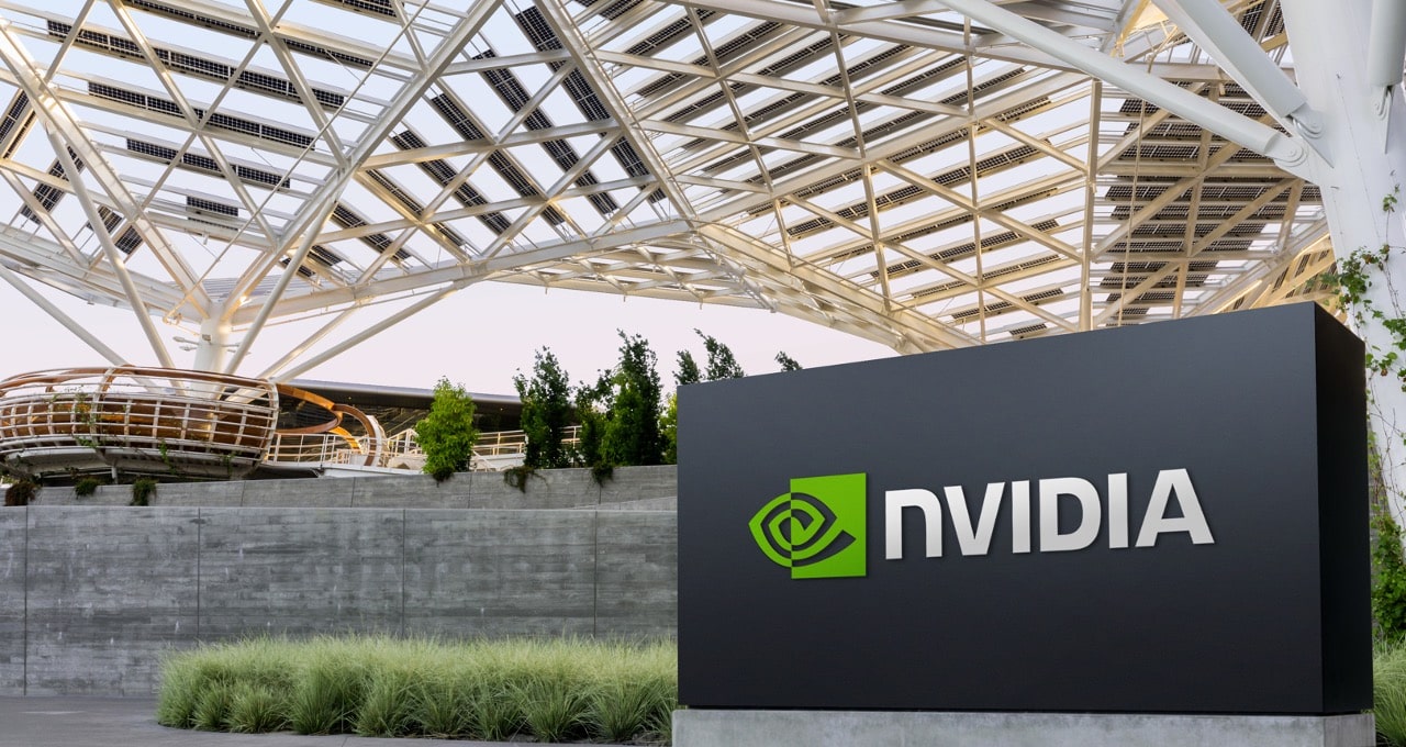
The Fabless Model: Nvidia’s Core Strategy for Innovation
The semiconductor industry is bifurcated into two primary models: Integrated Device Manufacturers (IDMs) like Intel, which design and manufacture their own chips, and the fabless model, pioneered by companies like Nvidia and Qualcomm. Nvidia’s strategic decision to remain fabless is central to its operational efficiency, innovation cycles, and market responsiveness.
What is a Fabless Company?
A fabless company specializes in the design and marketing of hardware devices, but does not own or operate a semiconductor fabrication plant (a “fab”). Instead, they rely on third-party foundries for the actual manufacturing of their integrated circuits. This model emerged in the late 20th century as the cost of building and maintaining state-of-the-art fabs skyrocketed into the tens of billions of dollars, making it impractical for every chip designer to own one. For Nvidia, this means focusing all its engineering prowess on architectural design, logic implementation, and the development of its CUDA software platform, which has become a crucial ecosystem for GPU acceleration across various computing paradigms.
Focusing on Design and Innovation
By shedding the enormous financial and operational burden of manufacturing, Nvidia can pour its resources into its core strengths: intellectual property (IP) development, advanced chip architecture, and software optimization. This strategy has enabled Nvidia to consistently push the boundaries of GPU technology, delivering generational leaps in performance, power efficiency, and specialized capabilities, particularly for AI and machine learning workloads. Their deep expertise in parallel computing and innovative chip designs, such as the Tensor Cores found in their latest GPUs, are direct outcomes of this focused approach. The ability to iterate rapidly on designs without the constraints of manufacturing cycles allows Nvidia to stay ahead in a fiercely competitive landscape.
Strategic Partnerships with Global Foundries
The success of the fabless model hinges entirely on robust, long-term partnerships with leading semiconductor foundries. These relationships are not merely transactional; they involve intricate collaborations, shared technological roadmaps, and significant R&D efforts. For Nvidia, two names stand out as its primary manufacturing partners: Taiwan Semiconductor Manufacturing Company (TSMC) and, to a lesser extent, Samsung Foundry. These foundries are technological powerhouses, investing heavily in the most advanced fabrication processes (measured in nanometers), which are critical for producing the densely packed, high-performance chips that Nvidia designs. The choice of foundry often depends on the specific product line, required process node, and strategic considerations regarding supply diversification.
Decoding the Semiconductor Manufacturing Process
Understanding where Nvidia chips are manufactured necessitates a glimpse into the labyrinthine process of semiconductor fabrication itself. This highly sophisticated journey transforms raw silicon into the complex integrated circuits that power our digital world.
From Sand to Silicon: The Journey Begins
The process starts not with sand, but with ultra-pure silicon crystals grown into large ingots. These ingots are then sliced into thin, circular wafers, which serve as the substrate for hundreds or thousands of individual chips. The wafers undergo an arduous series of steps in a cleanroom environment, where even a speck of dust can render a chip useless. These steps include deposition (adding thin layers of material), etching (removing material), and doping (introducing impurities to alter electrical properties). The most critical step is photolithography, where patterns of the chip’s intricate circuitry are projected onto the wafer using ultraviolet light, much like developing a photograph. This process is repeated dozens of times, layer upon layer, to build up the complex 3D structures of transistors and interconnects.
Advanced Fabrication Techniques
The relentless pursuit of smaller, more efficient transistors is at the heart of semiconductor innovation. This is often referred to by “node size,” such as 7nm, 5nm, or even 3nm, which broadly indicates the scale of the smallest features on the chip. Advanced fabrication techniques, like Extreme Ultraviolet (EUV) lithography, are indispensable for achieving these tiny dimensions, enabling billions of transistors to be packed onto a single die. Beyond mere transistor density, foundries are also innovating in areas like 3D stacking (where different layers of chips are stacked vertically to reduce interconnect length and improve performance) and advanced packaging solutions that integrate multiple components (e.g., CPU, GPU, memory) into a single package, improving overall system performance and power efficiency. These technological advancements are not proprietary to Nvidia but are developed by the foundries and offered as services to their fabless clients.
Quality Control and Testing
Throughout the manufacturing process, and especially at the final stages, rigorous quality control and testing are paramount. Each wafer is thoroughly inspected for defects. Once individual chips (dies) are cut from the wafer, they undergo electrical testing to ensure they meet performance specifications. Chips that fail are discarded, contributing to the “yield” metric—the percentage of functional chips from a wafer. This extensive testing ensures that only high-quality, fully functional chips make it to the subsequent stages of assembly and packaging, upholding Nvidia’s reputation for reliability and performance.
Key Global Foundries and Their Role

The geographical concentration of advanced semiconductor manufacturing is a critical aspect of the “where” in Nvidia’s production story.
TSMC: The Undisputed Leader
Taiwan Semiconductor Manufacturing Company (TSMC) is the undisputed global leader in advanced semiconductor manufacturing. Based in Hsinchu, Taiwan, TSMC has consistently been at the forefront of process technology, often being the first to mass-produce chips on the most advanced nodes (e.g., 7nm, 5nm, 4nm, and soon 3nm). Nvidia has relied heavily on TSMC for its flagship GPUs, including the highly sought-after chips for its GeForce RTX series, data center A100 and H100 GPUs, and professional Quadro cards. TSMC’s massive scale, technological leadership, and unparalleled expertise make it the go-to partner for companies like Nvidia that require bleeding-edge performance and high-volume production. The vast majority of Nvidia’s most advanced products are fabricated in TSMC’s state-of-the-art fabs located primarily in Taiwan, with increasing investments in other regions like Arizona, USA, and Japan.
Samsung Foundry: A Strong Contender
Samsung, a South Korean conglomerate, operates a robust foundry business (Samsung Foundry) that competes directly with TSMC. While not as dominant in market share for pure-play foundry services, Samsung Foundry offers highly competitive process technologies and has secured significant contracts from major chip designers, including some for Nvidia’s products. For instance, certain generations or segments of Nvidia’s GPU lineup have utilized Samsung’s manufacturing processes, offering Nvidia a degree of supply chain diversification and leveraging Samsung’s expertise, particularly in areas like memory integration (given Samsung’s leading position in memory manufacturing). This dual-sourcing strategy helps Nvidia mitigate risks associated with relying on a single foundry and can provide flexibility in production capacity. Samsung’s primary foundry operations are based in South Korea, with expansion efforts globally, including a significant fab under construction in Taylor, Texas, USA.
Other Players and Emerging Capacity
While TSMC and Samsung dominate the advanced nodes crucial for Nvidia, other foundries play roles in the broader semiconductor ecosystem. Intel, traditionally an IDM, is increasingly offering its manufacturing services through Intel Foundry Services (IFS) to external customers, aiming to become a major player in the foundry market. While Nvidia has not publicly announced a partnership with IFS for its leading-edge GPUs, the emergence of more foundry options could provide additional diversification opportunities in the future. GlobalFoundries, primarily based in the US and Europe, focuses on more mature process nodes, which are still vital for a vast array of specialized chips but not typically for Nvidia’s high-end GPUs. China also has its own domestic foundries, such as SMIC, which are developing advanced capabilities, though they currently lag behind TSMC and Samsung in leading-edge process technology.
Beyond the Wafer: Assembly, Testing, and Packaging (ATP)
The manufacturing journey of an Nvidia chip doesn’t conclude once the wafer leaves the foundry. A crucial “back-end” process follows, involving assembly, testing, and packaging, which prepares the raw silicon die for integration into electronic devices.
The Back-End Process Explained
After the wafers are fabricated at a foundry, they are sent to Outsourced Semiconductor Assembly and Test (OSAT) companies. Here, the wafers are cut into individual dies. Each die is then carefully mounted onto a substrate (a small circuit board), and microscopic wires are bonded to connect the die’s contact points to the substrate. This entire assembly is then encapsulated in a protective package, which can range from standard plastic casings to highly complex multi-chip modules that integrate the GPU die with high-bandwidth memory (HBM) stacks. This packaging not only protects the delicate silicon but also facilitates electrical connections to the wider system board and helps dissipate heat.
Global ATP Hubs
The global supply chain for ATP services is distinct from wafer fabrication. Many of the world’s leading OSAT companies are headquartered and operate substantial facilities in Southeast Asia. Countries like Malaysia, Singapore, Vietnam, Thailand, and the Philippines, along with China, have become major hubs for semiconductor assembly, testing, and packaging. These regions offer a combination of skilled labor, established infrastructure, and cost-effectiveness. Therefore, while an Nvidia chip might be fabricated in Taiwan or South Korea, its final assembly and testing could easily take place in Malaysia before being shipped to an original equipment manufacturer (OEM) to be integrated into a graphics card, laptop, or server.
Supply Chain Resiliency and Geopolitics
The geographically distributed nature of the semiconductor supply chain, while offering specialization and efficiency, also introduces vulnerabilities. Events like natural disasters (earthquakes, floods), global pandemics, and geopolitical tensions can significantly disrupt the flow of components, leading to shortages and impacting product availability. The recent global chip shortage underscored these fragilities. As a result, Nvidia, along with the broader industry and governments, is increasingly focused on supply chain resiliency, including efforts to diversify manufacturing locations and build redundancies to mitigate future disruptions. This involves strategic investments and collaborations to ensure a more robust and adaptable supply chain capable of withstanding various global challenges.
The Implications for Technology and Geopolitics
The intricate global manufacturing landscape of Nvidia’s chips has profound implications that extend beyond business strategy, touching upon national security, technological leadership, and future economic development.
Supply Chain Vulnerabilities and Dependencies
The heavy reliance on a few key players, particularly TSMC for advanced nodes, creates single points of failure within the global tech supply chain. A major natural disaster in Taiwan, for instance, or escalating geopolitical tensions in the region, could have catastrophic consequences for the supply of leading-edge chips, impacting everything from consumer electronics to critical infrastructure and defense systems. This dependency is not unique to Nvidia but is a systemic vulnerability for the entire tech industry that relies on advanced silicon.
The Drive for Domestic Manufacturing
In response to these vulnerabilities and as a matter of national security and economic competitiveness, several governments, most notably the United States and the European Union, have initiated significant policy drives and financial incentives to encourage domestic semiconductor manufacturing. Programs like the U.S. CHIPS and Science Act and similar initiatives in Europe aim to bring more fabrication capacity within their borders. This push is seeing foundries like TSMC and Samsung investing billions in new fabs in the US (Arizona and Texas, respectively) and Europe, creating a more geographically diversified manufacturing footprint, albeit at a higher cost. These efforts seek to reduce reliance on distant supply chains and ensure access to critical technologies in times of crisis.
Future Trends in Semiconductor Manufacturing
Looking ahead, the manufacturing landscape for companies like Nvidia will continue to evolve rapidly. We can expect continued innovation in advanced materials, new transistor architectures (like Gate-All-Around FETs), and more sophisticated packaging techniques (such as chiplets and heterogeneous integration) that allow different components to be optimally manufactured and then combined. Automation and AI are also increasingly being integrated into fab operations to boost efficiency and yield. Furthermore, sustainability is becoming a critical consideration, with efforts to reduce the immense water and energy consumption associated with chip manufacturing. As Nvidia continues to push the boundaries of AI and high-performance computing, its ability to leverage and influence these future manufacturing trends will be paramount to its ongoing success and leadership in the tech industry. The “where” of Nvidia’s manufacturing will thus remain a dynamic and strategically vital aspect of the global technological ecosystem.
aViewFromTheCave is a participant in the Amazon Services LLC Associates Program, an affiliate advertising program designed to provide a means for sites to earn advertising fees by advertising and linking to Amazon.com. Amazon, the Amazon logo, AmazonSupply, and the AmazonSupply logo are trademarks of Amazon.com, Inc. or its affiliates. As an Amazon Associate we earn affiliate commissions from qualifying purchases.