
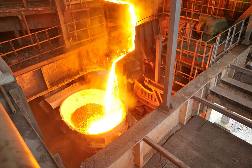
In the traditional sense, a “foundry” refers to a factory that produces metal castings. It is a place of heat, raw materials, and precision molds where molten metal is transformed into essential components for heavy industry. However, in the 21st century, the term has undergone a radical digital transformation. Today, when we ask “what does foundry mean?” in a technological context, we are referring to the bedrock of our digital existence: the massive facilities that manufacture the microchips powering our world and the sophisticated software platforms that “forge” raw data into actionable intelligence.
In the tech sector, a foundry represents the bridge between abstract design and physical reality. Whether it is a semiconductor fab producing 3-nanometer processors or a data foundry integrating disparate enterprise systems, the concept remains the same: a specialized environment where complex, raw inputs are refined into high-value outputs.
The Silicon Core: Semiconductor Foundries and the Fabless Model
The most prominent use of the term “foundry” today is in the semiconductor industry. A semiconductor foundry (commonly referred to as a “fab”) is a factory where integrated circuits (ICs) are manufactured. To understand the significance of the silicon foundry, one must first understand the “fabless” revolution that redefined how technology is built.
The Rise of Pure-Play Foundries
In the early days of computing, companies like Intel and IBM were Integrated Device Manufacturers (IDMs). They designed their own chips and manufactured them in their own factories. However, as the complexity of chip architecture grew, the cost of building and maintaining a fabrication plant became astronomical—often exceeding $20 billion for a single facility.
This led to the “Pure-Play Foundry” model, pioneered by companies like TSMC (Taiwan Semiconductor Manufacturing Company). These foundries do not design their own chips; instead, they manufacture chips for “fabless” companies like Apple, NVIDIA, and AMD. This specialization allows the foundry to focus exclusively on the physics and chemistry of manufacturing, while the designers focus on architecture and software.
The Process of Forging Silicon
The manufacturing process within a tech foundry is one of the most complex human endeavors. It begins with a silicon wafer, which undergoes hundreds of steps involving photolithography, etching, and chemical vapor deposition. Modern foundries utilize Extreme Ultraviolet (EUV) lithography to print features on chips that are measured in nanometers—sizes smaller than a human virus. When we say a foundry is at the “leading edge,” we mean it has the technological capability to produce these incredibly dense and efficient transistors.
Foundries as the Backbone of AI
The current explosion in Artificial Intelligence (AI) is entirely dependent on foundry capacity. High-performance GPUs, such as those designed by NVIDIA, require specialized foundry processes (like TSMC’s CoWoS packaging) to handle the massive data throughput needed for Large Language Models. Without the foundry, the “AI Revolution” would exist only as theoretical mathematics; the foundry provides the physical muscle required to run the code.
Software as a Foundry: The Evolution of Data Infrastructure
While hardware foundries deal with atoms and silicon, a new category of “Software Foundries” has emerged to deal with bits and data. In this context, a foundry is a centralized platform designed to integrate, manage, and “forge” data from dozens of different sources into a unified operating picture.
Palantir Foundry and Data Integration
The most notable example of this nomenclature is Palantir Foundry. In this technological framework, the term “foundry” describes a platform that allows large organizations to take “raw” data—which is often messy, siloed, and inconsistent—and pass it through a rigorous pipeline to create a “digital twin” of their operations.
Just as a metal foundry uses a mold to give shape to liquid iron, a software foundry uses data models to give shape to abstract information. This allows engineers and analysts to build applications, run simulations, and make decisions based on a single, high-fidelity source of truth.
The Role of Data Engineering Pipelines
Within a software foundry, the “manufacturing” process involves data cleaning, transformation, and ontological mapping. This ensures that a data point from a supply chain sensor in Malaysia is perfectly compatible with a sales figure from a retail outlet in London. By treating data as a raw material that must be “smelted” and “refined,” tech foundries enable enterprises to move beyond simple analytics into the realm of predictive modeling and automated decision-making.

Enabling Enterprise AI at Scale
A software foundry acts as the “operating system” for modern enterprises. By providing the infrastructure to manage data lineage and security, these platforms allow companies to deploy AI tools safely. You cannot have effective AI without a solid data foundation; the foundry provides that foundation, ensuring that the models are trained on high-quality, “refined” information rather than digital sludge.
The Mechanics of Precision: Inside the Advanced Fab
To truly appreciate what a tech foundry represents, one must look at the extreme environments required to produce modern technology. The physical foundry is perhaps the most controlled environment on Earth, pushing the limits of physics and engineering.
Cleanroom Environments and Contamination Control
In a semiconductor foundry, the presence of a single speck of dust can ruin a batch of microchips. Foundries operate “Class 1” cleanrooms, which contain fewer than one particle of dust per cubic foot of air. Employees wear “bunny suits” and undergo rigorous decontamination processes. This level of precision is what defines the “foundry” in the tech era—it is an environment where the margin for error is effectively zero.
The Advancement of Node Technology
The term “foundry” is often linked to “nodes,” such as 7nm, 5nm, or 3nm. These numbers historically referred to the size of the transistor gate, but today they serve as shorthand for the density and efficiency of the chip. As foundries move to smaller nodes, they use “FinFET” or “Gate-All-Around” (GAA) transistor architectures. Each leap in node technology requires a complete overhaul of the foundry’s equipment, costing billions of dollars in Research and Development (R&D).
Specialized Foundries and Legacy Nodes
Not all foundries focus on the smallest, fastest chips. There is a massive “Specialized Foundry” market that produces chips for the automotive and industrial sectors. These chips might use older “legacy nodes” (like 28nm or 65nm) but are designed for extreme durability, high voltages, or specific radio frequencies. This diversity highlights that a tech foundry is not just about raw power, but about the specific application of material science to solve technical problems.
The Strategic Importance: Geopolitics and Sovereign Foundries
In recent years, the meaning of “foundry” has transcended technology to become a matter of national security and global strategy. Because almost every modern device—from smartphones to fighter jets—depends on chips, the location and control of foundries have become a primary concern for world leaders.
The “Silicon Shield” and Geographic Concentration
A significant portion of the world’s leading-edge foundry capacity is concentrated in a few geographic locations, most notably Taiwan. This concentration has led to the concept of the “Silicon Shield,” where the global importance of a single foundry (TSMC) acts as a deterrent against geopolitical conflict. When a foundry is the only place on Earth capable of producing a specific type of technology, it becomes more than a factory; it becomes a global utility.
The Push for Sovereign Foundries
In response to supply chain vulnerabilities, regions like the United States and the European Union are investing hundreds of billions of dollars (via the CHIPS Act) to build “Sovereign Foundries.” The goal is to bring the “forge” back home, ensuring that the critical components of the tech economy are produced within domestic borders. This shift emphasizes that the foundry is the foundational unit of modern economic power.
Sustainability and the Future of Fabrications
As foundries grow in size and power, their environmental impact is coming under scrutiny. High-tech foundries require massive amounts of water and electricity. The “Foundry of the Future” is being redesigned with sustainability in mind, utilizing closed-loop water systems and renewable energy to power the lasers and cooling systems required for chip production. The meaning of “foundry” is thus evolving to include “stewardship,” as these facilities must balance the demands of cutting-edge tech with the realities of resource management.

Conclusion: The Foundry as the Forge of the Future
When we ask “what does foundry mean,” we are asking about the origin point of the modern world. In the tech sector, a foundry is where ideas become reality. It is the place where the laws of physics are manipulated to create silicon chips, and where the chaos of big data is structured into actionable software.
The foundry is the ultimate expression of human precision. Whether it is a multi-billion dollar cleanroom facility in Hsinchu or a sophisticated data integration platform used by a Fortune 500 company, the foundry serves as the essential infrastructure of the digital age. As we move further into the eras of Artificial Intelligence, quantum computing, and the Internet of Things, the role of the foundry will only become more central. It is the forge where the future is being shaped, one transistor and one data point at a time.
aViewFromTheCave is a participant in the Amazon Services LLC Associates Program, an affiliate advertising program designed to provide a means for sites to earn advertising fees by advertising and linking to Amazon.com. Amazon, the Amazon logo, AmazonSupply, and the AmazonSupply logo are trademarks of Amazon.com, Inc. or its affiliates. As an Amazon Associate we earn affiliate commissions from qualifying purchases.