
In the intricate world of modern technology, few questions are as fundamental and revealing as “Who makes the chips?” While Advanced Micro Devices (AMD) is a household name, synonymous with cutting-edge processors and graphics cards, the answer to who physically fabricates their silicon marvels is less straightforward than one might assume. Far from being a vertically integrated giant that designs and manufactures everything in-house, AMD operates on a “fabless” model, a strategic choice that has reshaped the semiconductor landscape and propelled innovation. Understanding who makes AMD chips requires diving deep into a complex, highly specialized global ecosystem of foundries, material scientists, and assembly partners, all working in concert to bring digital power to life. This article will unravel the layers of this ecosystem, focusing on the key players and processes that transform AMD’s groundbreaking designs into tangible products that power our digital world.
The Fabless Model: AMD’s Strategic Approach to Chip Design
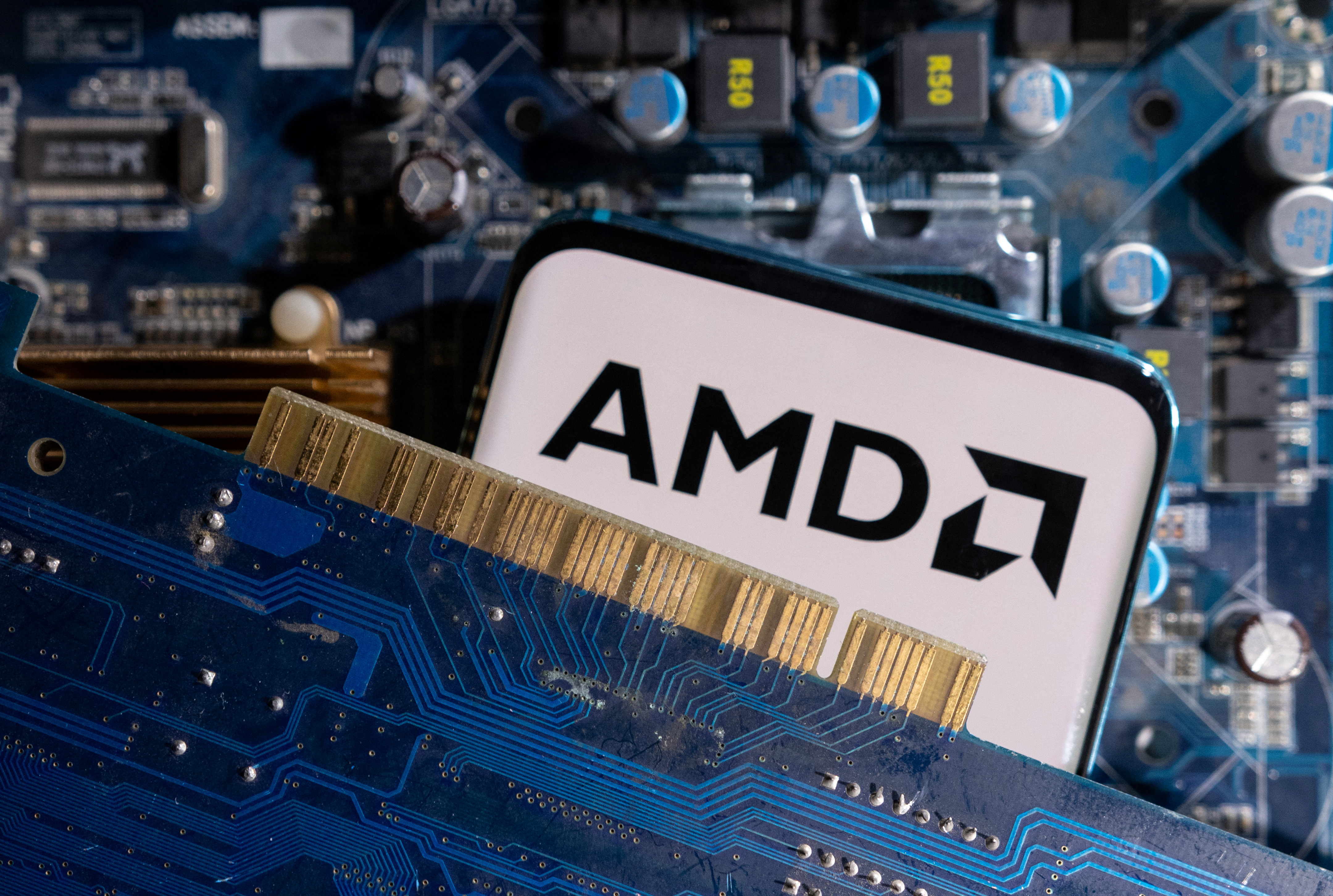
AMD’s success story in recent decades is inextricably linked to its embrace of the fabless business model. This strategic decision allows the company to focus its considerable resources on innovation, design, and intellectual property development, rather than the incredibly capital-intensive and rapidly evolving realm of semiconductor manufacturing.
Understanding the Fabless Semiconductor Company
A “fabless” semiconductor company, as the name suggests, is one that designs and sells hardware devices and semiconductor chips but does not own or operate a semiconductor fabrication plant (a “fab”). Instead, these companies outsource the actual manufacturing of their chip designs to specialized third-party foundries. This model contrasts sharply with “integrated device manufacturers” (IDMs) like Intel, which historically designed, manufactured, and sold their chips all under one roof. The fabless model began gaining traction in the 1980s and 1990s as the cost and complexity of building and maintaining cutting-edge fabs skyrocketed, making it economically unfeasible for many companies to sustain both design and manufacturing leadership simultaneously.
Advantages of the Fabless Model
The benefits of the fabless model for a company like AMD are profound. Firstly, it significantly reduces capital expenditure. Building and equipping a state-of-the-art semiconductor fab can cost tens of billions of dollars, with ongoing maintenance and upgrade costs in the billions annually. By outsourcing manufacturing, AMD avoids these colossal investments, freeing up capital to invest in research and development, talent acquisition, and market expansion. Secondly, it allows AMD to focus intensely on its core competencies: chip architecture, design, and software optimization. This specialized focus enables them to push the boundaries of performance, efficiency, and feature sets for their CPUs, GPUs, and APUs. Finally, the fabless model offers flexibility and scalability. AMD can choose from various foundries based on their technological capabilities, cost structures, and capacity, adapting swiftly to market demands and leveraging the most advanced process nodes available without being tied to the lifecycle or limitations of their own manufacturing facilities. This agility has been crucial in AMD’s recent resurgence and its ability to compete effectively against larger, more established players.
The Core of AMD’s Innovation
At its heart, AMD’s value proposition lies in its intellectual property and innovative designs. From the Zen microarchitecture that powers its Ryzen and Epyc processors to the RDNA architecture behind its Radeon graphics cards, AMD’s engineers are responsible for creating the blueprints, logic, and intricate layouts that define the performance and capabilities of their chips. This focus on design allows AMD to attract and retain world-class talent, fostering a culture of innovation that continuously challenges the status quo in computing and graphics. The physical chip itself is merely the manifestation of this design brilliance, brought to life by the manufacturing prowess of their foundry partners.
The Giants Behind the Silicon: Contract Semiconductor Foundries
While AMD designs its chips, the heavy lifting of physically producing them from raw silicon wafers falls to a select group of highly advanced contract semiconductor foundries. These are the unsung heroes of the tech world, investing massive sums in cutting-edge facilities and processes to fabricate the tiny, intricate transistors that power our devices.
TSMC: The Undisputed Leader in Advanced Manufacturing
Taiwan Semiconductor Manufacturing Company (TSMC) stands as AMD’s primary and most crucial manufacturing partner for its leading-edge processors and GPUs. Often referred to as the “foundry to the world,” TSMC is a pure-play foundry, meaning it exclusively manufactures chips for other companies and does not design its own. Its technological leadership and manufacturing scale are unparalleled, making it the preferred choice for companies like AMD, Apple, Qualcomm, and Nvidia seeking the most advanced process nodes.
TSMC’s dominance stems from its relentless pursuit of shrinking transistor sizes – measured in nanometers (nm) – which directly translates to more transistors on a chip, leading to greater performance, higher energy efficiency, and smaller chip sizes. AMD has heavily relied on TSMC’s 7nm, 5nm, and increasingly 3nm process technologies for its flagship Ryzen CPUs, Epyc server processors, and Radeon graphics cards. These advanced nodes require extraordinary precision, complex lithography techniques (including extreme ultraviolet or EUV lithography), and multi-billion-dollar investments in research and development and manufacturing equipment. TSMC’s consistent ability to deliver high yields and timely production on these cutting-edge nodes has been a critical factor in AMD’s ability to challenge Intel and Nvidia in recent years.
GlobalFoundries and Other Key Players
While TSMC handles AMD’s most advanced products, other foundries have played or continue to play roles in AMD’s broader portfolio, particularly for less leading-edge components or older generations of products.
GlobalFoundries (GF) has a unique and intertwined history with AMD. GlobalFoundries was actually spun off from AMD’s own manufacturing operations in 2009. For several years, AMD was legally bound by a “wafer supply agreement” to purchase a significant portion of its chips from GlobalFoundries. However, as TSMC pulled ahead in advanced process technology, AMD eventually amended these agreements to gain more flexibility, allowing it to move its high-performance products to TSMC. Today, GlobalFoundries still manufactures some of AMD’s products, primarily focusing on more mature nodes for components like I/O dies, specialized chiplets, and older generation processors or graphics cards that don’t require the absolute latest in transistor density. GlobalFoundries has pivoted its strategy to focus on differentiated technologies rather than chasing the bleeding edge of transistor size, serving diverse markets.
Samsung Foundry is another significant player in the contract manufacturing space, fiercely competing with TSMC for advanced nodes. While Samsung Foundry has secured major contracts with companies like Qualcomm and Nvidia for certain products, AMD’s primary allegiance for its core CPU and GPU products remains with TSMC due to historical relationships, process maturity, and capacity. However, the competitive landscape is dynamic, and foundry relationships can shift based on technology roadmaps, pricing, and geopolitical considerations.
The Intricate Journey: From Design to Finished Product
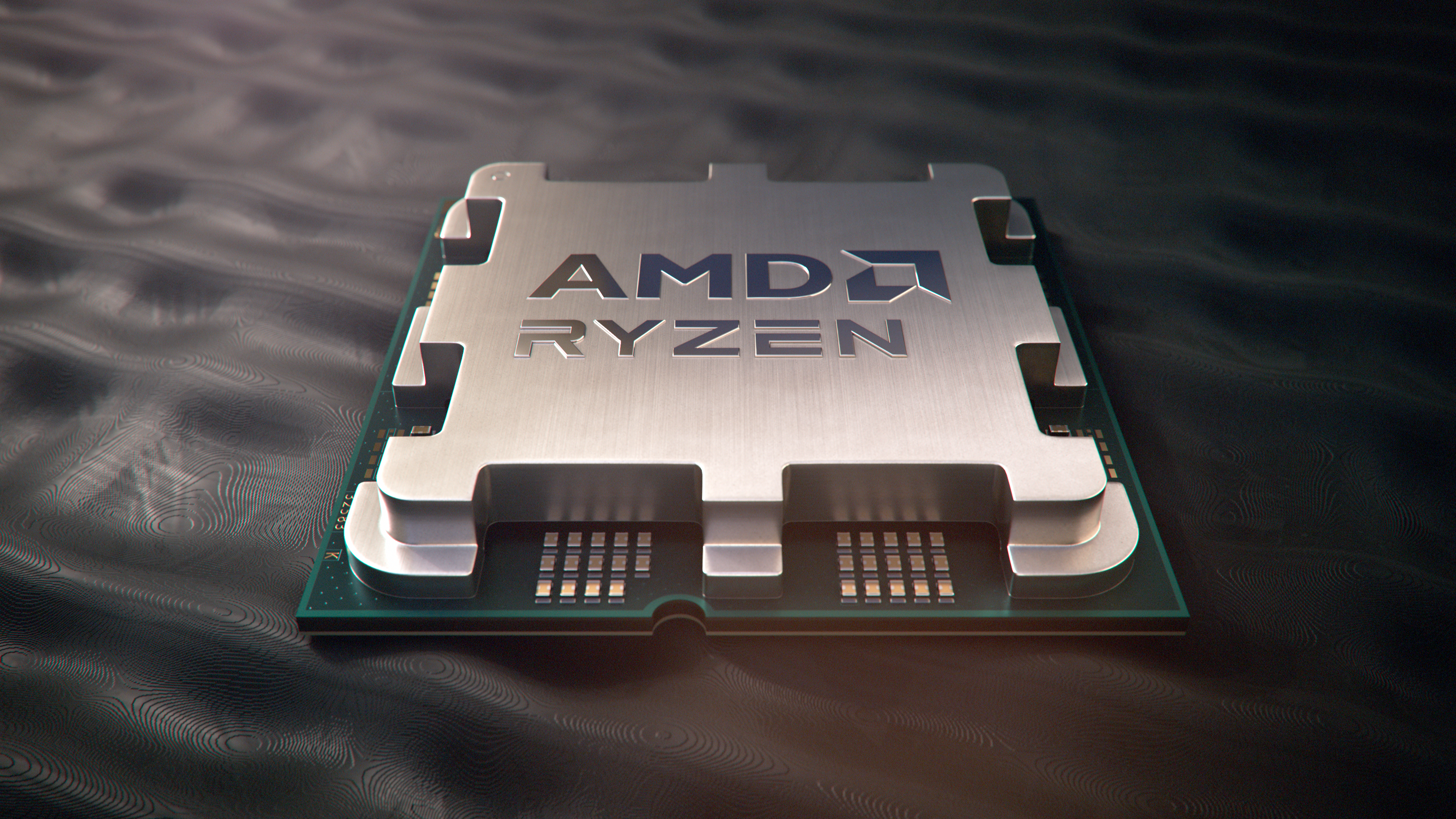
The journey of an AMD chip from a conceptual design to a functional product in your computer is a marvel of modern engineering and global logistics, involving numerous specialized steps and collaborative efforts.
Design and Architecture by AMD
The process begins at AMD’s design centers around the world. Here, teams of electrical engineers, computer architects, and software developers conceptualize the next generation of processors and GPUs. They define the instruction sets, memory controllers, cache structures, graphics pipelines, and myriad other components that will make up the chip. Using sophisticated electronic design automation (EDA) tools, they translate these architectural ideas into detailed circuit layouts, known as GDSII files. These files are essentially the digital blueprints, specifying the exact placement and connection of billions of transistors and interconnects on the silicon wafer. This is AMD’s core intellectual property, painstakingly crafted over years of research and development.
Wafer Fabrication: The Foundry’s Expertise
Once AMD finalizes its design, these GDSII files are sent to a chosen foundry, typically TSMC for its leading-edge products. The foundry then embarks on the highly complex process of wafer fabrication. This involves taking pristine, ultra-pure silicon wafers (thin discs of crystalline silicon) and subjecting them to hundreds of sequential steps in cleanroom environments, which are up to 10,000 times cleaner than a surgical operating room.
Key steps in wafer fabrication include:
-
Photolithography: Using specialized machines (steppers or scanners, increasingly employing EUV lithography), circuit patterns from masks (photomasks) are projected onto the wafer, coated with a light-sensitive material called photoresist.
-
Etching: Unprotected areas of the wafer are removed chemically or with plasma, transferring the pattern from the photoresist onto the silicon.
-
Deposition: New layers of material (conductors, insulators) are added to the wafer.
-
Doping: Impurities are intentionally introduced to create N-type and P-type semiconductor regions, forming transistors.
This cycle of deposition, lithography, etching, and doping is repeated dozens, sometimes hundreds, of times to build up the intricate, three-dimensional structure of transistors and interconnects that form the integrated circuit. Each wafer can contain hundreds or even thousands of individual chip dies.
Assembly, Testing, and Packaging (ATP)
After fabrication, the wafers contain many individual chip “dies” (the rectangular pieces of silicon that are the actual chips). These dies must then undergo several critical post-fabrication steps, often performed by specialized Outsourced Semiconductor Assembly and Test (OSAT) companies or, in some cases, by the foundries themselves.
-
Wafer Sort/Electrical Test: Each die on the wafer is tested to identify and mark any defective units, ensuring only functional dies proceed.
-
Dicing: The wafer is precisely cut into individual dies.
-
Die Attach: Good dies are mounted onto a substrate or lead frame.
-
Wire Bonding/Flip-Chip: Electrical connections are made between the die and the package using tiny wires or solder bumps (in the case of flip-chip technology, which is common for high-performance chips like AMD’s).
-
Packaging: The die and its connections are encapsulated in a protective package (e.g., LGA, BGA) that provides mechanical protection, heat dissipation, and a standardized interface for connection to a circuit board. This package also includes any necessary heat spreaders.
-
Final Test: The packaged chips undergo a comprehensive battery of tests to verify functionality, performance, power consumption, and thermal characteristics across various operating conditions. This is a critical step to ensure quality and adherence to specifications.
Quality Control and Supply Chain Management
Throughout this entire process, rigorous quality control measures are in place, from inspecting raw materials to final product validation. AMD works closely with its foundry and OSAT partners, sharing design data, testing protocols, and feedback to ensure that the manufactured chips meet its stringent quality and performance standards. Effective supply chain management is also paramount to coordinate the flow of wafers, dies, and finished products across different geographic locations and specialized facilities, minimizing delays and ensuring timely delivery to market.
The Impact and Future of Semiconductor Manufacturing
The complex interplay of design houses like AMD and manufacturing powerhouses like TSMC has profound implications, shaping the technological landscape and influencing global economics and geopolitics.
Geopolitical Implications and Supply Chain Resilience
The concentration of advanced semiconductor manufacturing in specific regions, particularly Taiwan (TSMC) and South Korea (Samsung), has become a significant geopolitical concern. This geographic concentration poses risks to global supply chains, as evidenced by disruptions caused by natural disasters, trade disputes, and the COVID-19 pandemic. Governments worldwide, recognizing the strategic importance of semiconductors, are now actively pursuing initiatives (like the CHIPS Act in the US and similar efforts in Europe) to onshore or friendshore semiconductor manufacturing capabilities, aiming to diversify supply chains and enhance national security. This push could lead to new fab construction in various countries, potentially altering the landscape of who makes chips in the coming decades.
The Race for Advanced Process Nodes
The relentless pursuit of smaller and more efficient transistors drives the entire semiconductor industry. Each new process node (e.g., from 7nm to 5nm to 3nm and beyond) represents a monumental leap in engineering, enabling chips to pack more processing power into smaller spaces while consuming less energy. This “Moore’s Law” phenomenon, though challenged, continues to fuel innovation in computing, artificial intelligence, and mobile technology. Foundries like TSMC and Samsung invest tens of billions annually in R&D and capital expenditures to stay at the forefront of this race, directly impacting AMD’s ability to deliver increasingly powerful and efficient products. The ability to access these leading-edge nodes is a key differentiator in the highly competitive semiconductor market.
Emerging Technologies and Future Collaborations
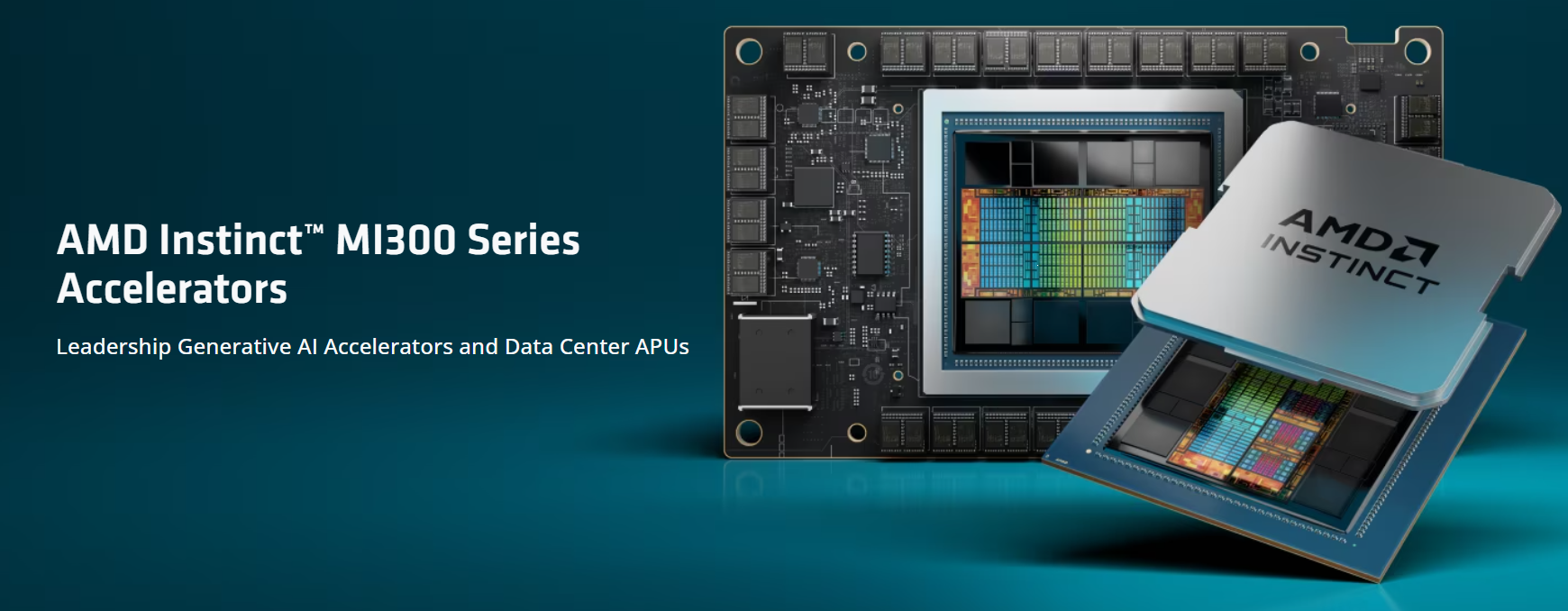
The future of semiconductor manufacturing is not just about shrinking transistors; it also involves advancements in packaging technologies (like 3D stacking and chiplets), new materials (e.g., gallium nitride, silicon carbide for specialized applications), and alternative computing paradigms (e.g., quantum computing). AMD has been a pioneer in chiplet-based designs, allowing it to mix and match different process nodes and IP blocks within a single package, further optimizing cost and performance. These innovations require even closer collaboration between fabless designers and their manufacturing partners, pushing the boundaries of what’s possible and ensuring that the semiconductor ecosystem remains vibrant and capable of meeting future technological demands.
In conclusion, while AMD designs and engineers its renowned chips, the actual fabrication is a collaborative masterpiece involving leading-edge foundries like TSMC. This strategic fabless model empowers AMD to focus on its core strength of innovation, leveraging the specialized manufacturing prowess of its partners. The complex journey from design blueprint to finished silicon underscores the interconnectedness and incredible technological sophistication of the modern semiconductor industry. As technology continues its rapid evolution, these symbiotic relationships will remain crucial, driving forward the digital revolution and bringing ever more powerful and efficient computing solutions to the world.
aViewFromTheCave is a participant in the Amazon Services LLC Associates Program, an affiliate advertising program designed to provide a means for sites to earn advertising fees by advertising and linking to Amazon.com. Amazon, the Amazon logo, AmazonSupply, and the AmazonSupply logo are trademarks of Amazon.com, Inc. or its affiliates. As an Amazon Associate we earn affiliate commissions from qualifying purchases.