
In the rapidly evolving landscape of modern electronics, the miniaturization of devices—from the sleek smartphone in your pocket to the high-performance servers powering the cloud—is made possible by a foundational manufacturing process known as Surface Mount Technology, or SMT. For anyone looking to understand how today’s gadgets achieve such high levels of complexity and performance within increasingly smaller footprints, understanding SMT is essential.
SMT refers to a method for producing electronic circuits in which the components are mounted or placed directly onto the surface of printed circuit boards (PCBs). This technology has largely replaced the older through-hole technology (THT) method, which involved fitting components with wire leads into holes drilled through the circuit board. By eliminating the need for these holes, SMT has revolutionized the speed, efficiency, and density of electronic manufacturing.

Understanding the Fundamentals of SMT
To appreciate the impact of SMT, one must first understand the shift it represented in industrial engineering. In the early days of electronics, components were bulky and required physical anchors through the board to ensure mechanical stability. SMT changed this paradigm by utilizing the surface of the board itself as the mounting plane.
From Through-Hole to Surface Mount
Before SMT became the industry standard in the 1980s, through-hole technology was the dominant assembly method. In THT, every component had “legs” or leads that had to be manually or semi-automatically inserted into pre-drilled holes and then soldered on the opposite side. While robust, this method was labor-intensive, required large components, and limited the amount of circuitry that could be placed on a single board because both sides of the board were effectively utilized by a single layer of components.
SMT solved these issues. By mounting components directly onto copper pads on the PCB surface, engineers could utilize both sides of the board for components. This effectively doubled the available real estate and allowed for the creation of much more complex circuits without increasing the physical size of the device.
The Rise of SMDs (Surface Mount Devices)
The components used in SMT are referred to as Surface Mount Devices (SMDs). Unlike their through-hole predecessors, SMDs are designed to be as small as possible. They often lack traditional wire leads, instead featuring small metallic tabs or solder balls on their underside that facilitate the connection to the PCB. Common SMDs include resistors, capacitors, integrated circuits (ICs), and transistors. The move toward SMDs has been the primary driver behind the “thinner and lighter” trend in consumer electronics over the last three decades.
The SMT Manufacturing Process: A Step-by-Step Overview
The transition to SMT was not just a change in component design; it required a complete overhaul of the manufacturing line. The SMT process is highly automated, relying on precision machinery to handle components that are often too small for the human eye to distinguish clearly.
Solder Paste Printing
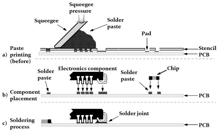
The process begins with the application of solder paste to the PCB. A stainless-steel stencil is placed over the board, aligning with the copper pads where the components will eventually sit. A squeegee then applies solder paste—a mixture of tiny solder particles and flux—through the stencil openings. This ensures that the exact amount of “glue” and conductive material is present to hold the component in place before it is permanently soldered.
Pick-and-Place: The Heart of Automation
Once the solder paste is applied, the board moves to the pick-and-place machine. This is perhaps the most impressive stage of the SMT line. Using high-speed robotic arms equipped with vacuum nozzles, the machine “picks” individual SMDs from reels or trays and “places” them onto the solder paste on the PCB.
Modern pick-and-place machines are incredibly fast and accurate, capable of placing tens of thousands of components per hour with micron-level precision. This level of automation is what allows manufacturers to produce millions of devices, such as motherboards or graphics cards, with minimal human intervention and high consistency.
Reflow Soldering
After the components are placed, they are held in position by the tackiness of the solder paste, but they are not yet electrically or mechanically secured. The board then passes through a reflow soldering oven. This oven contains multiple heating zones that gradually raise the temperature of the board.
In the peak temperature zone, the solder paste melts (reflows), creating a solid metallurgical bond between the component and the PCB pads. The board is then carefully cooled to solidify the joints. This process is delicate; if the heat is applied too quickly or unevenly, components can shift or “tombstone” (where one end lifts off the board), leading to a failed circuit.
Inspection and Quality Control
Given the density of modern PCBs, visual inspection by human eyes is often impossible. SMT lines utilize Automated Optical Inspection (AOI) systems. These systems use high-resolution cameras and sophisticated software to scan the boards for defects, such as missing components, bridge shorts, or misaligned parts. For more complex boards, such as those with Ball Grid Array (BGA) components where the connections are hidden underneath the chip, X-ray inspection is used to verify the integrity of the solder joints.

Why SMT Matters: Advantages for Modern Electronics
The adoption of SMT has been the single most important factor in the advancement of hardware technology. Its benefits span across performance, cost, and design flexibility.
Miniaturization and Space Efficiency
The most obvious benefit of SMT is size reduction. SMDs can be as small as 0.1mm by 0.05mm. Because SMT components do not require holes, they can be placed much closer together. Furthermore, the ability to populate both sides of a PCB allows designers to pack immense processing power into tiny enclosures. Without SMT, the modern smartphone would likely be the size of a briefcase.
Improved Electrical Performance
In high-frequency applications, such as 5G telecommunications or high-speed computing, the physical properties of the circuit matter immensely. Through-hole leads act as small inductors and capacitors, which can introduce “noise” or signal interference at high speeds. Because SMT components have very short leads or no leads at all, they have lower lead resistance and inductance. This results in better signal integrity and allows circuits to operate at much higher frequencies without degradation.
Cost-Effectiveness and Speed
While the initial setup for an SMT production line is expensive due to the sophisticated machinery required, the cost per unit in mass production is significantly lower than THT. The high level of automation reduces labor costs and increases throughput. Additionally, because the components are smaller and the boards require fewer drilled holes, the raw material costs for PCBs are reduced.
Challenges and Limitations of SMT
Despite its dominance, SMT is not without its challenges. The shift toward extreme miniaturization has introduced new hurdles for engineers and manufacturers.
Complexity of Repair and Rework
One of the primary drawbacks of SMT is that it is difficult, and sometimes impossible, to repair boards manually. While a through-hole resistor can be easily replaced with a standard soldering iron, an SMD requires specialized hot-air rework stations and microscopes. In many consumer electronics cases, it is more cost-effective to replace an entire module than to attempt a microscopic repair on a single failed SMT component.
Sensitivity to Mechanical Stress
Because SMT components are soldered directly to the surface, they are more susceptible to damage from mechanical stress or thermal expansion. If a PCB is flexed or subjected to extreme temperature swings, the solder joints can crack. Through-hole components, with their physical pins anchored through the board, tend to be more resilient in high-vibration environments, which is why THT is still occasionally used in heavy industrial or aerospace applications.
Thermal Management
As components get smaller and more densely packed, they generate significant heat in a concentrated area. Managing this thermal output is a major challenge for SMT designers. High-performance SMT boards often require complex cooling solutions, such as thermal vias (holes that conduct heat to internal copper layers) and sophisticated heat sinks, to prevent the components from overheating and failing.
The Future of SMT in the Age of AI and IoT
As we look toward the future of technology, SMT continues to evolve. The demands of Artificial Intelligence (AI), the Internet of Things (IoT), and wearable tech are pushing the boundaries of what is possible in manufacturing.
Industry 4.0 and Smart Manufacturing
The next generation of SMT lines is becoming smarter. By integrating AI and machine learning into the assembly process, machines can now predict when a nozzle is about to fail or adjust the solder paste volume in real-time based on environmental humidity. This “Smart Factory” approach minimizes waste and ensures near-perfect yield rates, which is critical as components become more expensive and harder to source.
The Push for Further Miniaturization
We are currently seeing the rise of “01005” and even smaller component sizes. These are so tiny that they resemble specks of dust to the naked eye. Handling these requires even more advanced pick-and-place technology and ultra-fine-pitch solder printing. As we move toward more integrated wearables and medical implants, the demand for this level of precision will only increase.
Sustainability and Lead-Free Soldering
The tech industry is also focusing on the environmental impact of SMT. For years, solder was primarily composed of lead, which posed environmental risks. Today, SMT has transitioned almost entirely to lead-free (RoHS compliant) materials. Current innovations focus on reducing the energy consumption of reflow ovens and developing recyclable PCB materials that can withstand the high temperatures of the SMT process.
Surface Mount Technology is the invisible force that has shaped the modern digital world. By transforming how we design and build electronic circuits, SMT has enabled the high-speed, high-density, and highly portable world we live in today. As technology continues to advance, the evolution of SMT will remain at the heart of every breakthrough in the hardware space.
aViewFromTheCave is a participant in the Amazon Services LLC Associates Program, an affiliate advertising program designed to provide a means for sites to earn advertising fees by advertising and linking to Amazon.com. Amazon, the Amazon logo, AmazonSupply, and the AmazonSupply logo are trademarks of Amazon.com, Inc. or its affiliates. As an Amazon Associate we earn affiliate commissions from qualifying purchases.