The modern technological landscape is defined by a silent, microscopic race for computational supremacy. At the center of this race stands Nvidia, a company that has evolved from a niche graphics card manufacturer into the backbone of the global Artificial Intelligence (AI) revolution. However, despite being a trillion-dollar titan of tech, Nvidia does not actually “make” its own physical products in the traditional sense. The question of where Nvidia chips are made reveals a complex, highly specialized, and geographically concentrated ecosystem that powers everything from GeForce gaming rigs to the massive H100 clusters training the next generation of Large Language Models.
To understand the geography of Nvidia’s production, one must first understand the “fabless” business model. Nvidia focuses its immense resources on research, development, and architectural design, while outsourcing the actual fabrication of the silicon wafers to specialized companies known as foundries. This article explores the technical nodes, the geographic hubs, and the advanced manufacturing processes that bring Nvidia’s designs to life.
The Fabless Model: Why Nvidia Doesn’t Build Its Own Fabs
The semiconductor industry is bifurcated into two main types of entities: Integrated Device Manufacturers (IDMs) like Intel, who both design and manufacture chips, and “fabless” companies like Nvidia, AMD, and Apple. Nvidia’s decision to remain fabless is a strategic one, rooted in the staggering technical and financial hurdles of modern silicon fabrication.
The Architecture vs. Assembly Divide
Nvidia’s core competency lies in the mathematical architecture of the Graphics Processing Unit (GPU). Their engineers design the intricate layouts of billions of transistors that must work in parallel to process complex data. Writing the “blueprints” for a chip like the Blackwell B200 architecture is an epic feat of software and electrical engineering. However, translating those blueprints into a physical object requires a cleanroom environment thousands of times cleaner than a surgical operating room and machinery that costs hundreds of millions of dollars per unit. By remaining fabless, Nvidia can pivot its architecture every two years without having to retool a multi-billion dollar factory.
Strategic Partnerships with Foundries
Because Nvidia does not own factories, it relies on deep, multi-year technical partnerships with foundries. These are not mere “customer-client” relationships; they are collaborative engineering efforts. When Nvidia designs a chip for a “4nm” or “3nm” process, they must work closely with the foundry to ensure the design is physically manufacturable. This synergy is the reason why the location of Nvidia’s chips is synonymous with the locations of its primary partners.
The Heart of the Operation: Taiwan Semiconductor Manufacturing Company (TSMC)
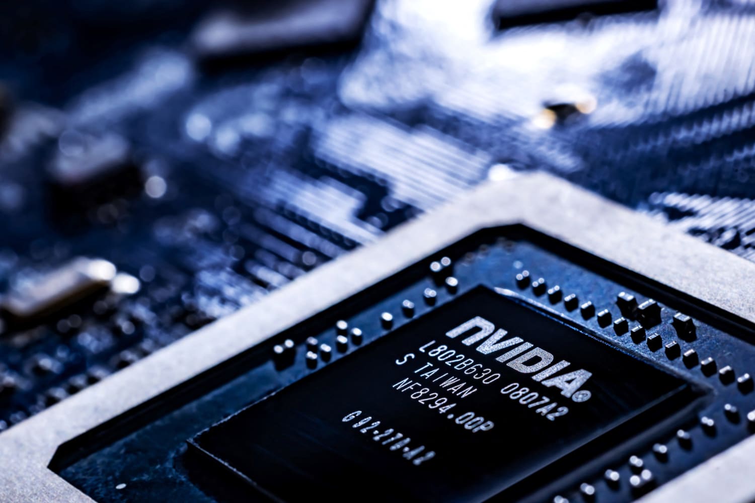
When discussing where Nvidia chips are made, the conversation begins and ends largely with one company: TSMC. Based in Taiwan, TSMC is the most advanced semiconductor manufacturer in the world, and it is the sole producer of Nvidia’s most critical high-end AI and data center chips.
The Hsinchu Science Park and Beyond
The vast majority of Nvidia’s high-performance silicon is birthed in Taiwan, specifically within the Hsinchu Science Park and the Southern Taiwan Science Park in Tainan. TSMC’s “GigaFabs” are the sites where Nvidia’s flagship products, such as the A100, H100, and the newer Blackwell series, are etched onto 300mm silicon wafers. These facilities are the only places on Earth currently capable of producing the volumes and yields required for Nvidia’s global supply chain.
Advanced Process Nodes: The EUV Revolution
The technical “where” is just as important as the geographic “where.” Nvidia chips are manufactured using Extreme Ultraviolet (EUV) lithography. This technology uses light with incredibly short wavelengths to “print” transistor gates that are only a few nanometers wide. TSMC’s mastery of the 5nm (N5) and 4nm (N4) nodes has been the primary reason Nvidia has maintained a lead over competitors. By utilizing TSMC’s advanced nodes in Taiwan, Nvidia achieves higher transistor density, which translates directly into the massive TFLOPS (Teraflops) of compute power required for modern AI training.
Beyond Taiwan: Diversifying the Technical Footprint
While TSMC is the primary engine, Nvidia has historically utilized other foundries to balance its supply chain and manage costs, particularly for its consumer-grade gaming GPUs.
The Role of Samsung Electronics
For the GeForce RTX 30-series (the Ampere architecture), Nvidia famously moved a significant portion of its production to Samsung Electronics’ foundries in South Korea. Samsung utilized an 8nm process for these chips. While Taiwan remains the hub for the highest-performance enterprise silicon, South Korea serves as a vital secondary node in Nvidia’s manufacturing map. This diversification allows Nvidia to navigate capacity constraints at TSMC, although the company has recently leaned back toward TSMC for the 40-series and AI chips due to TSMC’s superior power efficiency at smaller nodes.
Intel Foundry Services: A Future Contender?
In the tech world, the manufacturing map is constantly shifting. Nvidia CEO Jensen Huang has publicly expressed openness to using Intel’s manufacturing facilities in the future. Intel is currently investing heavily in its “Intel Foundry” business, building new fabs in Ohio and Arizona. If Intel can prove its “18A” process node is competitive with TSMC, we may soon see “Made in the USA” Nvidia chips appearing in data centers, representing a major shift in the global tech supply chain.
The Global Assembly Line: Packaging and Testing
The manufacturing of an Nvidia chip does not end once the silicon wafer is etched. A raw die is useless until it is “packaged”—connected to a substrate, surrounded by memory, and protected by a heat spreader. This stage of the process, known as OSAT (Outsourced Semiconductor Assembly and Test), adds more locations to the Nvidia map.
CoWoS Technology and Advanced Packaging
The AI revolution has moved the bottleneck from chip fabrication to chip packaging. Nvidia’s H100 chips use a specialized TSMC technology called CoWoS (Chip-on-Wafer-on-Substrate). This process allows Nvidia to mount HBM (High Bandwidth Memory) directly alongside the GPU die on a single silicon interposer. Most of this advanced packaging still happens in Taiwan at specialized TSMC facilities, but it also involves partners like ASE Technology.
The Geographic Footprint of Backend Operations
Once the chips are packaged, they move to testing and assembly facilities. These “backend” operations are more geographically dispersed than the “frontend” fabrication. Nvidia utilizes facilities in Malaysia, China, and Vietnam for various stages of testing and final board assembly. While the “brain” of the chip is a product of Taiwanese high-tech lithography, the final graphics card or server blade is a truly global product, often crossing several borders before reaching the end user.
The Geopolitical Tech Race and the Future of Production
The high concentration of Nvidia’s manufacturing in Taiwan has become a focal point of global tech strategy. As AI becomes a matter of national security, the “where” of chip making is undergoing a massive transformation.
The CHIPS Act and Onshoring Efforts
In response to the fragility of global supply chains, the U.S. government passed the CHIPS and Science Act, providing billions in incentives to bring semiconductor manufacturing back to American soil. TSMC is currently building massive fabrication plants in Phoenix, Arizona. These facilities are slated to produce 4nm and 3nm chips—the exact specifications required for Nvidia’s future hardware. This means that within the next few years, a significant portion of Nvidia’s production will likely shift to the United States.
Technological Sovereignty in the AI Era
The move toward onshoring and “friend-shoring” is driven by the need for technological sovereignty. Europe is also attempting to attract foundries through its own European Chips Act, with Intel planning facilities in Germany. For Nvidia, this means a more resilient, albeit more expensive, manufacturing footprint. The future of Nvidia chips will be defined by a shift from a Taiwan-centric model to a distributed global network of high-tech fabs located in the US, Europe, and Asia.
Conclusion: A Masterpiece of Global Engineering
In summary, when we ask “where are Nvidia chips made,” the answer is a testament to human ingenuity and global cooperation. The architectural genius happens in Santa Clara, California. The physical creation occurs in the ultra-advanced cleanrooms of Hsinchu and Tainan, Taiwan. The secondary production cycles through South Korea, while the final assembly and testing span across Southeast Asia.
As Nvidia continues to push the boundaries of what is possible with silicon, the “where” will continue to evolve. From the transition to 2nm nodes to the opening of new frontiers in the American desert, the production of an Nvidia chip remains the most complex technical workflow in the history of industry. It is a process that requires the perfect alignment of light, chemistry, and global logistics to produce the silicon hearts that are currently defining the future of intelligence.
aViewFromTheCave is a participant in the Amazon Services LLC Associates Program, an affiliate advertising program designed to provide a means for sites to earn advertising fees by advertising and linking to Amazon.com. Amazon, the Amazon logo, AmazonSupply, and the AmazonSupply logo are trademarks of Amazon.com, Inc. or its affiliates. As an Amazon Associate we earn affiliate commissions from qualifying purchases.