Processors, the brains behind our digital lives, are marvels of modern engineering. From the smartphone in your pocket to the supercomputer crunching complex data, these intricate chips are responsible for executing commands and powering our ever-increasing reliance on technology. But what exactly are these microscopic powerhouses crafted from? Dive with us into the fascinating world of processor materials, exploring the fundamental elements and sophisticated processes that bring them to life, and how this impacts the broader landscape of tech innovation and even business strategy.
The Silicon Heartbeat: The Foundation of Modern Processors
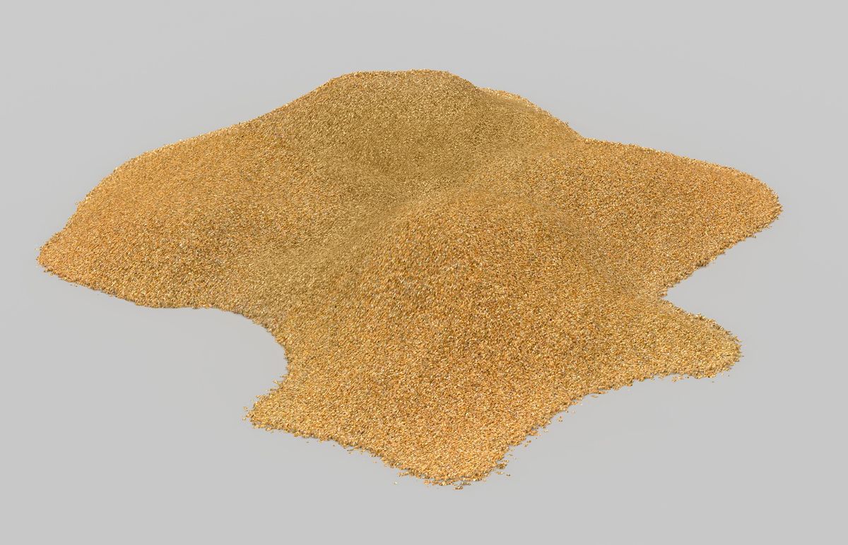
At its core, the material that forms the backbone of virtually all modern processors is silicon. This abundant semiconductor element, extracted from sand and quartz, possesses a unique electrical property: it can conduct electricity, but its conductivity can be precisely controlled. This control is paramount for the billions of microscopic switches, known as transistors, that make up a processor.
From Sand to Semiconductor: The Purification Process
The journey of silicon from a common mineral to a high-purity semiconductor is a testament to advanced material science and chemical engineering.
-
Extraction and Refining: The process begins with extracting silicon dioxide (silica) from sand or quartz. This raw material is then subjected to intense heat in an electric arc furnace with carbon. This reduces the silica to metallurgical-grade silicon, which is about 98-99% pure. While this is pure enough for some industrial applications, it’s far from sufficient for the exacting demands of microelectronics.
-
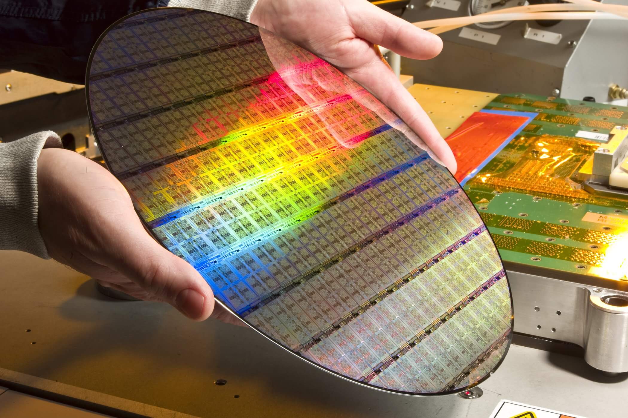
Zone Refining and Crystal Growth: To achieve the incredibly high purity required for semiconductor applications – often exceeding 99.9999999% – a process called zone refining is employed. In this method, a molten zone is passed along a rod of polycrystalline silicon. As the zone moves, impurities are preferentially carried with it, leaving behind a much purer silicon crystal. The result is a purified silicon ingot. This ingot is then melted again and slowly pulled from the molten state using a seed crystal. This controlled cooling and solidification process forms a single, large, cylindrical crystal of silicon, known as a monocrystalline silicon ingot. These ingots can be several feet long and weigh hundreds of pounds.
Doping: Imbuing Silicon with Electrical Properties
Pure silicon, while a semiconductor, doesn’t inherently possess the conductivity needed for complex circuits. This is where the crucial process of doping comes into play. Doping involves intentionally introducing tiny amounts of specific impurity atoms into the silicon crystal lattice. These impurity atoms have a different number of valence electrons than silicon (which has four), altering the silicon’s electrical conductivity in predictable ways.
-
N-type Silicon: When atoms with five valence electrons, such as phosphorus or arsenic, are introduced, they donate an extra electron to the silicon lattice. This creates an excess of free electrons, making the silicon “n-type” (negative charge carriers).
-
P-type Silicon: Conversely, when atoms with three valence electrons, like boron or gallium, are introduced, they create “holes” – the absence of an electron – in the silicon lattice. These holes can accept electrons, effectively acting as positive charge carriers. This makes the silicon “p-type” (positive charge carriers).
The precise arrangement and combination of n-type and p-type silicon regions within a processor are what create the millions or billions of transistors that perform logical operations.
Beyond Silicon: Exotic Materials and Their Roles
While silicon remains the dominant material, the relentless pursuit of higher performance, greater efficiency, and new functionalities in processors is driving research and adoption of other materials. These advanced materials are crucial for overcoming the limitations of silicon and enabling the next generation of computing.
The Rise of III-V Semiconductors
Materials from Groups III and V of the periodic table, such as gallium arsenide (GaAs) and indium gallium arsenide (InGaAs), are gaining prominence, particularly in high-frequency applications and specialized chips.
-
Advantages over Silicon: These materials boast significantly higher electron mobility than silicon. This means electrons can travel through them much faster, leading to faster switching speeds and thus higher clock frequencies in processors. This is particularly beneficial for radio frequency (RF) applications found in wireless communication devices and for high-performance computing where speed is paramount.
-
Challenges and Applications: However, III-V semiconductors are generally more expensive to produce and more fragile than silicon. They are also more difficult to integrate into large-scale manufacturing processes. Despite these challenges, they are finding their way into specialized processors for high-speed networking, advanced communication systems, and some high-performance integrated circuits where their speed advantage justifies the cost.
Carbon-Based Innovations: Graphene and Carbon Nanotubes
The remarkable electrical and thermal properties of carbon have positioned it as a potential successor or complementary material to silicon.
-
Graphene: A single layer of carbon atoms arranged in a hexagonal lattice, graphene exhibits incredibly high electron mobility, superior thermal conductivity, and exceptional mechanical strength. Its potential lies in creating even faster and more energy-efficient transistors. Researchers are exploring methods to integrate graphene into processor designs, aiming to push the boundaries of speed and miniaturization beyond what silicon can offer.
-
Carbon Nanotubes (CNTs): These cylindrical molecules of carbon can also exhibit excellent electrical conductivity and mechanical properties. They can be used as nanowires or as the channel material in transistors. The challenge with CNTs lies in their consistent manufacturing and precise placement on a chip, which is an ongoing area of intensive research.
Emerging Technologies: Quantum Computing Materials
For the realm of quantum computing, entirely different materials and phenomena are at play. While not traditional processors in the silicon sense, these systems rely on quantum bits (qubits) that can exist in multiple states simultaneously.
-
Superconducting Materials: Some quantum computers utilize superconducting materials like niobium or aluminum. At extremely low temperatures, these materials lose all electrical resistance, enabling the precise manipulation of quantum states.
-
Trapped Ions and Photons: Other quantum computing approaches use individual atoms (trapped ions) or photons as the basis for qubits. These systems often involve complex laser systems and magnetic fields to control and read out the quantum information, with the underlying materials playing a supporting role in creating the trapping and manipulation environments.
The Manufacturing Ballet: From Raw Material to Functional Chip
The transformation of these raw materials into the sophisticated processors we use daily is a breathtakingly complex and precise process, involving hundreds of steps executed in highly controlled environments. This manufacturing process, often referred to as fabrication, is a cornerstone of the technology industry and a significant driver of economic activity.
The Fabrication Plant (Fab) Environment
Processor fabrication takes place in specialized facilities known as “fabs” or “semiconductor foundries.” These are among the cleanest environments on Earth, with strict controls over dust particles, temperature, and humidity. Even a single speck of dust can render a processor useless.
-
Cleanrooms: Fabs employ “cleanrooms” where the air is filtered thousands of times per minute. Workers wear specialized suits, including hairnets, masks, and full body coverings, to minimize contamination.
-
Photolithography: The Art of Patterning: The core of the fabrication process is photolithography. This technique uses light to transfer circuit designs from a mask onto the silicon wafer.
- Wafer Preparation: A purified silicon wafer, typically 12 inches in diameter, serves as the substrate.
- Layer Deposition: Various materials, including insulators (like silicon dioxide) and conductors (like copper or aluminum), are deposited onto the wafer in thin layers.
- Photoresist Coating: A light-sensitive material called a photoresist is applied to the wafer.
- Exposure: Ultraviolet (UV) light is shone through a mask (containing the circuit pattern) onto the photoresist. The exposed areas of the photoresist undergo a chemical change.
- Development: The exposed or unexposed photoresist is then chemically removed, leaving behind a patterned layer of photoresist that protects certain areas of the wafer.
- Etching: Chemical or plasma etching is used to remove the underlying material in the areas not protected by the photoresist, thus creating the intricate patterns of the circuit.
- Stripping: The remaining photoresist is then removed.
-
Doping and Ion Implantation: Following patterning, doping is performed through processes like ion implantation, where charged impurity atoms are accelerated and embedded into specific regions of the silicon wafer.
-
Interconnects and Metallization: Multiple layers of transistors are built up, and then incredibly thin wires made of materials like copper or aluminum are deposited and patterned to connect these transistors, forming the complex circuitry.
Testing and Packaging: Ensuring Quality and Functionality
Once the fabrication of the intricate circuits on the wafer is complete, a rigorous process of testing and packaging begins.
-
Wafer Testing (Electrical Die Sort): Before the wafer is cut into individual chips, each die (individual processor) on the wafer undergoes electrical testing to identify any defects or non-functional units. Defective dies are marked.
-
Dicing: The wafer is then cut into individual dies using a diamond saw or a laser.
-
Packaging: The functional dies are then mounted into protective casings, known as packages. This packaging not only protects the delicate silicon die but also provides the electrical connections to the outside world. These connections are made through pins or solder balls on the underside of the package, allowing the processor to be mounted onto a motherboard.
-
Final Testing: The packaged processors undergo a final round of thorough testing to ensure they meet all performance specifications and quality standards.
The Economic and Strategic Implications
The materials used in processors, the complexity of their manufacturing, and the constant drive for innovation have profound economic and strategic implications across the technology sector and beyond.
The Global Semiconductor Supply Chain
The production of processors is a global endeavor, with different regions specializing in various stages. For example, the raw silicon might be purified in one country, fabricated into wafers and chips in another (often East Asia), and then packaged and tested elsewhere. This intricate and geographically dispersed supply chain is vital for the global economy but also presents vulnerabilities. Geopolitical tensions and natural disasters can disrupt this delicate balance, leading to shortages and price fluctuations.
The Arms Race of Innovation and Moore’s Law
The continuous evolution of processor materials and manufacturing techniques is driven by the pursuit of ever-increasing performance and efficiency. This is famously encapsulated by Moore’s Law, which observes the doubling of transistors on a microchip roughly every two years. While the literal interpretation of Moore’s Law is becoming increasingly challenging due to physical limits, the spirit of relentless innovation continues. Companies invest billions in research and development to discover new materials, refine manufacturing processes, and design more sophisticated architectures. This innovation race fuels the entire tech industry, from software development to AI advancements, and influences product design and market competitiveness.

Brand Identity and Technological Leadership
For technology companies, the ability to design and manufacture cutting-edge processors is a significant differentiator and a key component of their brand identity. Companies known for their powerful and efficient processors often command premium pricing and customer loyalty. This technological leadership is built on years of investment in materials science, engineering talent, and manufacturing infrastructure. The materials used and the performance achieved by their processors become a testament to their engineering prowess and their commitment to pushing the boundaries of what’s possible. Understanding what processors are made of, and the innovation driving their evolution, is therefore not just a technical curiosity but a critical insight into the competitive landscape of the modern technology-driven economy.
aViewFromTheCave is a participant in the Amazon Services LLC Associates Program, an affiliate advertising program designed to provide a means for sites to earn advertising fees by advertising and linking to Amazon.com. Amazon, the Amazon logo, AmazonSupply, and the AmazonSupply logo are trademarks of Amazon.com, Inc. or its affiliates. As an Amazon Associate we earn affiliate commissions from qualifying purchases.