In the vast and intricate world of digital electronics, where every operation, from the simplest calculator function to the most complex artificial intelligence algorithm, breaks down into binary code—zeros and ones—the humble logic gate stands as a fundamental building block. Among these essential components, the NAND gate holds a particularly distinguished position. Far from being a mere curiosity, the NAND gate is a ubiquitous element, forming the bedrock of modern computing and digital systems. Understanding its function is key to grasping how microprocessors process information, how memory stores data, and how virtually all digital devices operate at their most basic level.

The Foundational Logic of Digital Electronics
To fully appreciate the significance of a NAND gate, it’s crucial to first understand the foundational principles of Boolean logic, which governs all digital circuits. Developed by George Boole in the mid-19th century, Boolean algebra provides a mathematical framework for analyzing and designing logic circuits by representing true/false conditions as binary values, typically 1 and 0.
Understanding Boolean Logic
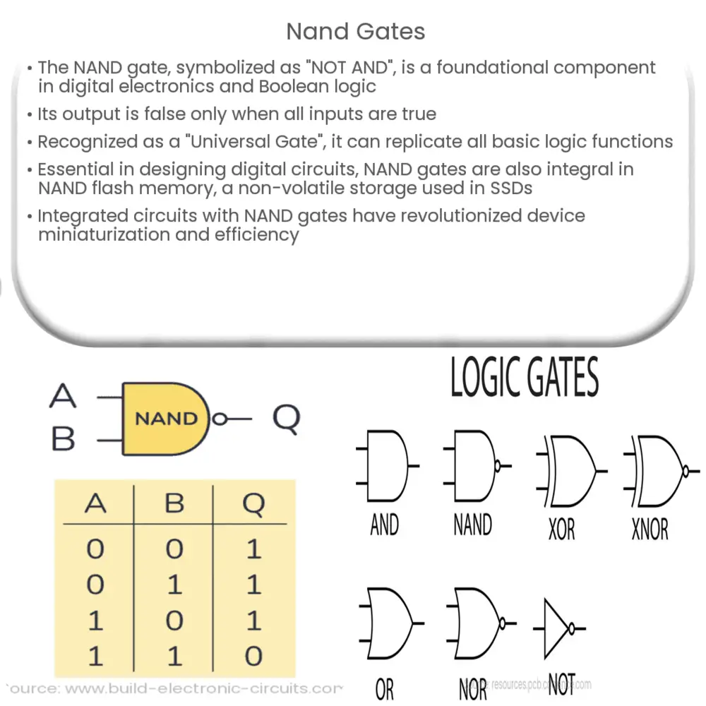
At the heart of Boolean logic are basic operations that manipulate these binary inputs to produce binary outputs. The most fundamental gates are the AND, OR, and NOT gates.
- AND Gate: Outputs a 1 (true) only if all its inputs are 1 (true). Otherwise, it outputs a 0 (false).
- OR Gate: Outputs a 1 (true) if at least one of its inputs is 1 (true). It only outputs a 0 (false) if all inputs are 0 (false).
- NOT Gate (Inverter): Takes a single input and reverses it. If the input is 1, the output is 0; if the input is 0, the output is 1.
These basic gates are the logical primitives. However, practical digital circuit design often leverages more complex gates that combine these basic operations. The NAND gate is one such combination, essentially an “AND” operation followed by a “NOT” operation.
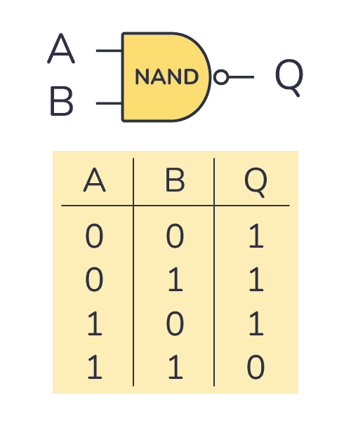
Definition and Symbolism
A NAND gate, an acronym for “NOT-AND,” is a digital logic gate that produces an output that is false (0) only if all its inputs are true (1). In all other cases, the output is true (1). This direct inversion of the AND function gives it unique properties and immense utility.
Its standard circuit symbol is easily recognizable: it looks like an AND gate symbol but with a small circle (often called an “inversion bubble”) at its output. This bubble universally denotes an inversion or negation of the preceding logic function. For a 2-input NAND gate, if the inputs are A and B, the output (Y) can be expressed in Boolean algebra as Y = (overline{A cdot B}), where the dot signifies the AND operation and the bar above signifies the NOT (inversion) operation.
How a NAND Gate Operates
The operation of a NAND gate, like all digital logic gates, is fundamentally tied to the behavior of transistors, which act as high-speed electronic switches. While the abstract logic provides the conceptual understanding, the physical implementation dictates how these gates function in real-world integrated circuits.
Transistor-Level Implementation
In modern silicon-based microchips, NAND gates are predominantly constructed using Complementary Metal-Oxide-Semiconductor (CMOS) technology. A typical 2-input CMOS NAND gate employs a combination of p-type (pMOS) and n-type (nMOS) transistors.
Consider a 2-input NAND gate:
- nMOS Transistors: Two nMOS transistors are connected in series between the output and ground. nMOS transistors conduct (turn ON) when their gate voltage is high (1).
- pMOS Transistors: Two pMOS transistors are connected in parallel between the output and the positive power supply (Vcc). pMOS transistors conduct (turn ON) when their gate voltage is low (0).
Here’s how the various input combinations affect the output:
- Inputs A=0, B=0: Both pMOS transistors are ON, creating a path from Vcc to the output, pulling the output HIGH (1). Both nMOS transistors are OFF, blocking the path to ground.
- Inputs A=0, B=1: One pMOS is ON, the other OFF. One nMOS is OFF, the other ON. The parallel pMOS connection ensures a path to Vcc, so the output remains HIGH (1). The series nMOS connection blocks the path to ground.
- Inputs A=1, B=0: Similar to the above, one pMOS is OFF, the other ON. One nMOS is ON, the other OFF. The parallel pMOS connection keeps the output HIGH (1). The series nMOS connection blocks the path to ground.
- Inputs A=1, B=1: Both pMOS transistors are OFF. Both nMOS transistors are ON, creating a path from the output to ground, pulling the output LOW (0).
This transistor-level understanding reveals the elegant interplay of semiconductor physics that translates binary inputs into a precise binary output according to the NAND logic.
Input-Output Relationship (Truth Table)
The behavior of any logic gate is completely defined by its truth table, which lists all possible input combinations and their corresponding output. For a 2-input NAND gate:
| Input A | Input B | Output Y = (overline{A cdot B}) |
|---|---|---|
| 0 | 0 | 1 |
| 0 | 1 | 1 |
| 1 | 0 | 1 |
| 1 | 1 | 0 |
As evident from the table, the output is only 0 when both inputs A and B are 1. In all other scenarios, where at least one input is 0, the output is 1. This “NOT-AND” characteristic makes the NAND gate remarkably versatile.
The Universal Gate: Building Any Logic Function
Perhaps the most compelling reason for the NAND gate’s prominence is its property as a “universal gate.” This means that any other basic logic gate—AND, OR, NOT, XOR, XNOR—can be constructed solely using NAND gates. This universality significantly simplifies the manufacturing and design of complex digital circuits.
Why NAND is “Universal”
The ability to construct all other gates from a single type of gate offers immense practical advantages in integrated circuit (IC) fabrication. Instead of needing different types of fundamental gates on a chip, engineers can rely exclusively on NAND gates, streamlining the production process, reducing material costs, and simplifying design rules.
Here’s how other gates can be built using only NAND gates:
- NOT Gate: If the two inputs of a NAND gate are tied together (A=B), the output becomes (overline{A cdot A} = overline{A}). Thus, a single NAND gate with shorted inputs acts as an inverter.
- AND Gate: An AND gate can be formed by taking the output of a NAND gate and feeding it into another NAND gate configured as an inverter (a NAND-NOT combination). So, (overline{overline{A cdot B}} = A cdot B).
- OR Gate: An OR gate can be constructed by inverting each input individually with NAND gates (as NOT gates) and then feeding these inverted signals into a final NAND gate. This applies De Morgan’s theorem: (overline{overline{A} cdot overline{B}} = A + B).
- NOR Gate: Similar to the OR gate, a NOR gate is an OR gate followed by an inverter. So, once an OR gate is formed by NANDs, its output can be fed into a NAND-based inverter to achieve the NOR function.
- XOR and XNOR Gates: While more complex, these can also be constructed entirely from combinations of NAND gates. For instance, an XOR gate can be realized using four NAND gates.
Practical Implications of Universality
The universality of the NAND gate has profound implications for semiconductor manufacturing and digital system design. It means that an IC designer only needs to master the optimization and fabrication of one type of fundamental gate to build entire microprocessors, memory chips, or complex control logic. This homogeneity leads to:
- Simplified Manufacturing: Production lines can be optimized for one gate type, improving yields and reducing complexity.
- Cost Reduction: Fewer distinct components lead to lower material and development costs.
- Compact Designs: By standardizing on NAND, engineers can achieve denser circuit layouts, contributing to the miniaturization of electronic devices.
- Enhanced Reliability: Using a single, well-understood gate type can lead to more robust and reliable designs.
Real-World Applications and Significance
The theoretical elegance and practical versatility of the NAND gate translate into its pervasive presence across virtually every digital technology we interact with daily. Its influence extends from the smallest embedded systems to the most powerful supercomputers.
Core of Modern Computing
NAND gates are indispensable components in:
- Microprocessors (CPUs): The complex arithmetic logic units (ALUs), control units, and registers within a CPU are built from millions, if not billions, of logic gates, with NAND gates being a primary constituent. They perform calculations, manage data flow, and execute instructions.
- Microcontrollers: These integrated circuits, which combine a CPU, memory, and input/output peripherals on a single chip, rely heavily on NAND logic for their internal operations and control functions in countless embedded applications (e.g., smart appliances, automotive systems).
- Memory Devices: Notably, NAND flash memory derives its name directly from the gate’s function. This non-volatile memory type, found in SSDs, USB drives, smartphones, and digital cameras, uses floating-gate transistors arranged in a NAND-like structure to store data. Each memory cell in a NAND flash array is effectively connected in series, and a specific logic (similar to a NAND operation) determines whether data can be read or written.
- Digital Signal Processing (DSP): Circuits that manipulate digital signals (like audio, video, or sensor data) for filtering, compression, or analysis leverage NAND gates as part of their logic to perform these complex operations.
Memory Cells and Latches
Beyond its role in processing, the NAND gate is fundamental to digital memory. Two cross-coupled NAND gates can form a basic SR (Set-Reset) Latch, which is a one-bit memory cell. This simple configuration can “remember” a state (0 or 1) indefinitely until a new signal actively changes it. SR latches are the building blocks for more sophisticated memory elements like D-type flip-flops, registers, and ultimately, the cache memory and RAM found in computers. Without these fundamental memory units constructed from gates like NAND, storing data in digital form would be impossible.
Robustness and Efficiency
In various semiconductor technologies, NAND gates often exhibit superior performance characteristics compared to other gates. They can be designed to be:
- Faster: Due to their specific transistor configurations, they can switch states very quickly.
- More Power-Efficient: In CMOS technology, NAND gates typically draw very little power when idle, as current only flows during state transitions.
- More Compact: Their symmetrical design often allows for denser packing on a silicon die, which is crucial for increasing the transistor count and computational power of modern ICs.
These advantages directly contribute to the relentless miniaturization of electronics and the continuous improvement in performance and battery life of our digital devices.
The Future of Logic Gates and Digital Design
As technology advances, pushing the boundaries of what’s possible with silicon, the fundamental principles of logic gates, including the NAND gate, remain remarkably consistent. While the scale shrinks and architectures evolve, the core idea of processing binary information through logical operations persists.
Evolution of Integrated Circuits
Moore’s Law, the observation that the number of transistors on a microchip doubles approximately every two years, has largely been sustained by continuous innovation in fabricating ever smaller and more efficient transistors. NAND gates have been at the forefront of this revolution, their optimized designs contributing to the incredible density and speed of modern processors and memory chips. Future generations of integrated circuits will continue to refine these designs, exploring new materials and manufacturing techniques to push performance further.
Beyond Traditional Silicon
While traditional silicon CMOS technology dominates today, research into emerging computing paradigms like quantum computing, neuromorphic computing, and spintronics is ongoing. Even in these radically different approaches, the need for fundamental logic operations endures. While a quantum computer might not have a physical “NAND gate” in the classical sense, the concept of performing a specific logical transformation on information remains central. The NAND gate, therefore, serves not just as a physical component, but as a universal conceptual primitive in the digital domain, influencing how we design and understand information processing, regardless of the underlying physical substrate. Its legacy as the ultimate building block for digital logic is secure, poised to inspire new forms of computation for decades to come.
aViewFromTheCave is a participant in the Amazon Services LLC Associates Program, an affiliate advertising program designed to provide a means for sites to earn advertising fees by advertising and linking to Amazon.com. Amazon, the Amazon logo, AmazonSupply, and the AmazonSupply logo are trademarks of Amazon.com, Inc. or its affiliates. As an Amazon Associate we earn affiliate commissions from qualifying purchases.