
The technological prowess that powers modern artificial intelligence, high-performance computing, and immersive gaming experiences largely stems from the sophisticated graphics processing units (GPUs) designed by Nvidia. Yet, the journey from conceptual design to a tangible, high-functioning chip is a global odyssey, a complex ballet performed across continents by an intricate network of specialized manufacturers. Nvidia itself does not own the massive fabrication plants (fabs) where its groundbreaking designs come to life; instead, it operates on a “fabless” model, leveraging the expertise and colossal investments of third-party foundries. Understanding where these critical components are manufactured illuminates the intricate global supply chain that underpins today’s digital world.

The Complex Global Supply Chain Behind Nvidia’s Dominance
Nvidia’s position at the forefront of the technology landscape is a testament to its innovation in chip design, particularly its GPUs, which have become the fundamental engines for everything from generative AI models to autonomous vehicles. However, the physical realization of these designs involves a highly specialized and distributed manufacturing ecosystem. The “fabless” business model adopted by Nvidia is central to this paradigm.
Fabless Model: Design vs. Production
In the fabless model, companies like Nvidia concentrate their resources entirely on research and development, architecture design, intellectual property creation, and software ecosystems. They are the architects of the chips, crafting the intricate blueprints for processors that will define the next generation of computing. This strategy allows them to avoid the astronomical capital expenditure required to build and maintain state-of-the-art semiconductor fabrication plants—facilities that can cost tens of billions of dollars to construct and hundreds of millions annually to operate and upgrade.
Instead of owning fabs, Nvidia contracts with specialized semiconductor foundries, which are companies solely dedicated to manufacturing chips for other firms. This division of labor allows Nvidia to remain agile and focused on innovation, while foundries achieve economies of scale and technical specialization by serving numerous fabless design houses. This symbiotic relationship has been a cornerstone of the semiconductor industry’s rapid advancement, fostering a global ecosystem where design leadership and manufacturing excellence can thrive independently yet collaboratively.
Key Manufacturing Partners: The Foundry Giants
At the heart of Nvidia’s manufacturing strategy are a select few foundry partners, global titans of semiconductor fabrication that possess the cutting-edge technology and sheer scale necessary to produce the most advanced chips. For Nvidia’s leading-edge GPUs, the primary and most critical manufacturing partner is Taiwan Semiconductor Manufacturing Company (TSMC). TSMC is unrivaled in its capacity and technological sophistication, producing a vast majority of the world’s most advanced chips, including those at the leading edge of transistor density and performance. While TSMC dominates, other foundries like Samsung Foundry in South Korea also play a role, particularly for certain product lines or older process technologies, contributing to a degree of supply chain diversification, albeit still highly concentrated.
Raw Materials and Upstream Components
Before even reaching the foundry, the journey of an Nvidia chip begins with an equally complex upstream supply chain. This involves the sourcing and refining of highly pure silicon, the fundamental substrate for all semiconductors, predominantly from countries like China, Japan, and the United States. Beyond silicon wafers, the manufacturing process relies on an extensive array of specialized chemicals, gases, photomasks, and advanced manufacturing equipment—each supplied by a global network of specialized vendors, many of whom are themselves monopolies or duopolies in their specific niche. The extreme purity and precision required for these materials and tools mean that even the most basic components of a chip are the product of significant global collaboration and technological expertise.
Taiwan Semiconductor Manufacturing Company (TSMC): The Core of Nvidia’s Production
When discussing the manufacturing location of Nvidia’s most advanced chips, one name stands preeminent: Taiwan Semiconductor Manufacturing Company (TSMC). Based primarily in Taiwan, TSMC is not just a foundry; it is the linchpin of the global technology supply chain, responsible for fabricating a substantial portion of the world’s most sophisticated semiconductors. For Nvidia, particularly its high-performance GPUs like those in the Hopper (H100) and Blackwell (B100) series crucial for AI, TSMC is the indispensable partner.
TSMC’s Technological Prowess and Scale
TSMC’s dominance stems from its relentless pursuit of advanced process technology. The company consistently invests tens of billions of dollars annually into research and development, along with constructing new fabs, pushing the boundaries of miniaturization and efficiency. They are the pioneers and masters of leading-edge process nodes—the numerical representation (e.g., 5nm, 4nm, 3nm) of the smallest feature size on a chip, directly correlating with transistor density, performance, and power efficiency. Nvidia relies heavily on these cutting-edge nodes to pack billions of transistors onto a single die, enabling the unparalleled parallel processing capabilities required for AI training and complex simulations.
TSMC’s scale is equally critical. Operating multiple “gigafabs” capable of processing hundreds of thousands of wafers per month, TSMC possesses the capacity to meet the immense demand for Nvidia’s chips, which are central to the explosive growth in AI and data centers. This scale, combined with their proprietary manufacturing processes and robust intellectual property portfolio, creates a formidable barrier to entry for competitors and solidifies their position as the go-to partner for companies requiring state-of-the-art silicon.
The Significance of Advanced Process Nodes
The ‘nm’ (nanometer) number associated with a chip’s manufacturing process node is a critical indicator of its sophistication. Smaller numbers imply that transistors are packed more densely, leading to more powerful, efficient, and smaller chips. Nvidia’s flagship GPUs utilize TSMC’s most advanced nodes—for instance, the Hopper H100 GPU is built on TSMC’s custom 4N process (a variant of their 5nm node), while future generations are slated for 3nm and beyond. This continuous march towards smaller process nodes is vital for Nvidia to maintain its performance lead, as each new generation allows for a significant leap in computational power and efficiency, directly impacting the capabilities of AI models and graphics rendering.
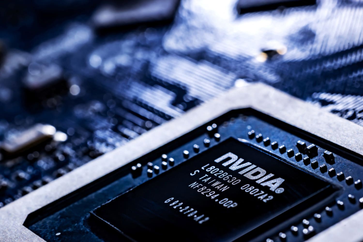
Geographic Concentration and Geopolitical Implications
The concentration of such critical manufacturing capabilities in Taiwan, an island nation with complex geopolitical dynamics, introduces significant global risk. The world’s reliance on TSMC for leading-edge semiconductors has created a “silicon shield,” but also highlights a critical vulnerability. Any disruption to TSMC’s operations—whether from natural disasters, power outages, or geopolitical events—would send shockwaves across the global technology industry, potentially halting the production of everything from smartphones and servers to advanced military equipment. This concentration has spurred global efforts by nations like the United States and European Union to encourage diversification and domestic chip manufacturing, recognizing the strategic importance of semiconductor supply chain resilience.
Beyond the Fab: Assembly, Testing, and Packaging (ATP)
While wafer fabrication in a foundry like TSMC is arguably the most complex and capital-intensive step, the journey of an Nvidia chip is far from complete when it leaves the fab. The raw wafers, still largely sheets of interconnected circuits, must undergo several crucial post-fabrication processes: Assembly, Testing, and Packaging (ATP). These steps transform the fabricated wafer into individual, usable chip packages that can be integrated into larger electronic systems.
Global ATP Hubs
The ATP segment of the semiconductor supply chain is typically more geographically distributed than wafer fabrication. While some foundries offer integrated ATP services, many fabless companies like Nvidia utilize specialized Outsourced Semiconductor Assembly and Test (OSAT) providers. These firms operate extensive facilities, often concentrated in Southeast Asia, particularly in countries like Malaysia, Vietnam, the Philippines, and China. Major OSAT players include ASE Technology Holding (Taiwan), Amkor Technology (USA, with operations globally), and Siliconware Precision Industries Co. (SPIL, Taiwan).
- Assembly: This stage involves dicing the wafer into individual chip “dies.” Each die is then mounted onto a substrate, usually a printed circuit board (PCB) or an interposer, and connected using incredibly fine wires (wire bonding) or solder bumps (flip-chip technology). For Nvidia’s high-performance AI GPUs, advanced packaging techniques like TSMC’s CoWoS (Chip-on-Wafer-on-Substrate) are employed. CoWoS allows multiple dies (e.g., the GPU die and high-bandwidth memory, HBM) to be integrated onto a single interposer, enabling incredibly fast communication and compact footprints—a critical enabler for modern AI accelerators.
- Testing: After assembly, each chip undergoes rigorous testing to ensure it meets performance specifications and is free from defects. This involves complex automated test equipment (ATE) that runs diagnostic routines and performance benchmarks on billions of transistors. Chips that fail are discarded, contributing to yield rates, while successful chips are graded based on their performance characteristics.
- Packaging: The final step encases the assembled and tested chip in a protective package (e.g., BGA – Ball Grid Array, QFN – Quad Flat No-leads) that protects it from environmental damage and provides a standardized interface for integration onto motherboards or other PCBs. The package also aids in heat dissipation, a crucial factor for powerful GPUs.
The Importance of Quality Control
Throughout the ATP process, stringent quality control measures are paramount. A single faulty connection or microscopic impurity can render an entire chip useless, impacting yield rates and increasing costs. Nvidia, through its close collaboration with OSAT partners, implements rigorous testing protocols and quality assurance checks at every stage to ensure that the final packaged GPUs meet its exacting standards for reliability and performance. The distributed nature of ATP, while offering some resilience through geographic spread, also necessitates robust logistical coordination and standardized quality benchmarks across multiple vendors and locations.
The Strategic Imperative: Diversification and Resilience
The unprecedented demand for semiconductors, particularly advanced chips for AI, coupled with the geopolitical realities surrounding their manufacturing, has ignited a global imperative for supply chain diversification and resilience. Nations and major tech companies alike are now actively seeking to mitigate the risks associated with the high concentration of leading-edge semiconductor production in a single region.
Onshoring and Friendshoring Initiatives
In response to these vulnerabilities, governments worldwide have launched ambitious initiatives to bolster domestic or regionally allied semiconductor manufacturing capabilities. The US CHIPS and Science Act is a prime example, committing over $50 billion to incentivize semiconductor research, development, and manufacturing within the United States. Similarly, the European Chips Act aims to double the EU’s share in global chip production to 20% by 2030, with significant investments in new fabs and R&D.
These efforts involve:
- Onshoring: Bringing manufacturing facilities back to the country where the designing company is headquartered or where the end-users are primarily located. Intel, for instance, is building new fabs in Ohio and Arizona. While Nvidia is fabless, its partners like TSMC are establishing new facilities in the US (Arizona) and Japan (Kumamoto), and potentially Europe, which contributes to localizing the fabrication for US and European-designed chips.
- Friendshoring: Locating manufacturing in geopolitically aligned or “friendly” nations to enhance supply chain security without necessarily being fully domestic. This strategy aims to reduce reliance on potentially adversarial regions while still leveraging global expertise and cost efficiencies.
Challenges and Costs of Diversification
While the strategic benefits of diversification are clear, the challenges and costs are immense. Building a state-of-the-art semiconductor fab can take several years and requires investments in the tens of billions of dollars. These facilities also demand a highly skilled workforce, from process engineers to specialized technicians, which can be scarce in many regions. Furthermore, the existing ecosystem of upstream suppliers—for chemicals, gases, and specialized equipment—is deeply entrenched in existing manufacturing hubs, making a complete shift extraordinarily difficult and costly. Environmental concerns, including water usage and energy consumption, also add layers of complexity to establishing new fab locations.

Impact on Future Technology Trends
The push for diversification will undoubtedly reshape the semiconductor landscape. For Nvidia, this means a potential future where its most advanced chips might be fabricated in multiple locations globally, perhaps by TSMC in Arizona, or by other foundries in Europe or South Korea, reducing single-point-of-failure risks. This increased resilience, while coming at a higher cost in the short term, could stabilize future technology development and availability. It will also foster greater collaboration and competition among regions, potentially accelerating innovation as new manufacturing hubs emerge. Ultimately, the question of “where” Nvidia chips are manufactured will likely have an increasingly diversified answer in the coming decades, reflecting a global consensus on the strategic necessity of a more robust and resilient semiconductor supply chain.
aViewFromTheCave is a participant in the Amazon Services LLC Associates Program, an affiliate advertising program designed to provide a means for sites to earn advertising fees by advertising and linking to Amazon.com. Amazon, the Amazon logo, AmazonSupply, and the AmazonSupply logo are trademarks of Amazon.com, Inc. or its affiliates. As an Amazon Associate we earn affiliate commissions from qualifying purchases.