Intel, a titan in the semiconductor industry, has long been synonymous with innovation in microprocessors. For decades, the company has not only designed its cutting-edge chips but also manufactured them in its own state-of-the-art facilities across the globe. This integrated approach, known as Integrated Device Manufacturing (IDM), has been a cornerstone of Intel’s strategy, allowing unparalleled control over the entire production process from design to fabrication. Understanding where Intel manufactures its chips is not merely a geographic exercise; it’s an exploration into the intricate, multi-billion-dollar world of semiconductor technology, global supply chains, and strategic geopolitical positioning that defines the modern tech landscape.

The manufacturing of a semiconductor chip is one of the most complex and capital-intensive endeavors known to humankind. It involves thousands of steps, ultra-clean environments, and highly specialized machinery, all orchestrated to create the microscopic circuits that power our digital world. Intel’s manufacturing footprint reflects this complexity, strategically located to leverage regional advantages, ensure supply chain resilience, and drive technological advancement.
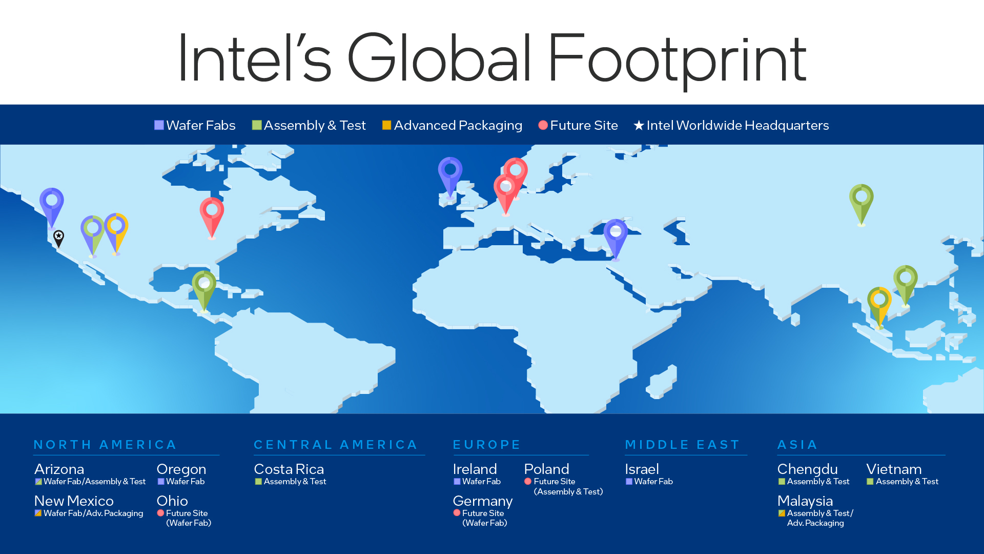
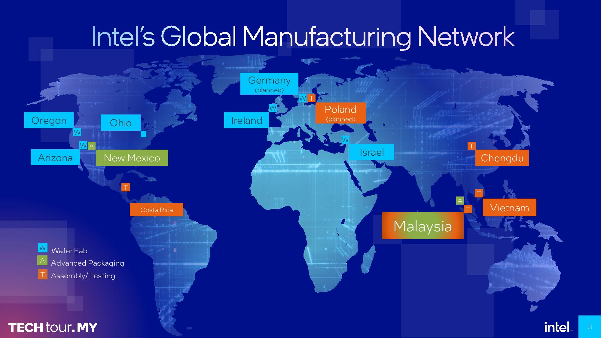
Intel’s Global Manufacturing Footprint: A Network of Advanced Fabs
Intel’s manufacturing operations are spread across several key regions worldwide, each hosting specialized facilities crucial to the chip production lifecycle. These facilities, primarily “fabs” (fabrication plants), are colossal, multi-story structures designed to maintain extreme cleanliness and house highly sophisticated equipment.
U.S. Operations: The Heart of Innovation and Core Fabrication
The United States remains a critical hub for Intel’s manufacturing and research and development (R&D) efforts. Historically, Intel’s roots are deeply embedded in Silicon Valley, and while much of the primary fabrication has expanded, significant operations persist.
- Oregon (Ronler Acres Campus, Hillsboro): This campus is arguably Intel’s most advanced R&D and manufacturing site globally. It serves as the primary location for developing new process technologies (e.g., Intel 4, Intel 3, Intel 20A, Intel 18A). Once a new process node is perfected in Oregon, it is then transferred to other high-volume manufacturing fabs for mass production. This site also includes some high-volume manufacturing capabilities for leading-edge products, effectively bridging R&D with initial production runs.
- Arizona (Ocotillo Campus, Chandler): Arizona is home to some of Intel’s most significant high-volume manufacturing fabs. These facilities are crucial for producing a vast array of Intel’s processors, from server CPUs to client processors. The Ocotillo campus has seen continuous expansion and investment, solidifying its role as a bedrock of Intel’s manufacturing capacity. Intel has announced further expansion plans in Arizona, including new fabs to boost domestic semiconductor production.
- New Mexico (Rio Rancho): While having undergone various transformations over the years, Intel’s facility in New Mexico traditionally specialized in advanced packaging technologies, including its innovative 3D stacking Foveros technology. This site plays a vital role in integrating multiple chiplets into a single package, enhancing performance and efficiency.
- Ohio (New Albany): A recent and significant addition to Intel’s U.S. manufacturing strategy is the planned “Ohio One” manufacturing campus in New Albany. This massive investment, projected to be one of the largest semiconductor manufacturing sites in the world, aims to boost domestic chip production dramatically and reinforce the U.S. position in leading-edge semiconductor manufacturing. It will host multiple fabs and is a cornerstone of Intel’s commitment to re-shoring and expanding its U.S. manufacturing capabilities.
These U.S. sites collectively represent Intel’s commitment to maintaining a strong domestic manufacturing base, crucial for both technological leadership and national security. They are at the forefront of developing and deploying the most advanced process nodes.
European Hubs: Precision, Proximity, and Strategic Expansion
Intel’s presence in Europe is characterized by advanced manufacturing and a growing strategic footprint, particularly important for serving European markets and diversifying supply chains.
- Ireland (Leixlip, County Kildare): Intel’s campus in Ireland is one of its largest and most advanced manufacturing sites outside the U.S. It boasts multiple fabs that produce leading-edge processors for a global market. Ireland has consistently attracted significant Intel investments due to a skilled workforce, favorable business environment, and strategic location. The Irish fabs are crucial for high-volume production of Intel’s latest silicon.
- Germany (Magdeburg, Saxony-Anhalt): Similar to the Ohio expansion, Intel has announced plans for a massive new mega-fab complex in Magdeburg, Germany. This project, part of the European Chips Act initiatives, aims to establish a leading-edge semiconductor manufacturing ecosystem in the heart of Europe. It signifies a major step towards bolstering European self-sufficiency in chip production and is a testament to Intel’s global expansion strategy.
These European sites highlight Intel’s dual objective: to continue producing high-tech chips efficiently and to play a pivotal role in strengthening regional semiconductor supply chains.
Asian Presence: Assembly, Test, and Packaging Expertise
While much of the complex wafer fabrication takes place in the U.S. and Europe, Asia plays a critical role in the later stages of chip manufacturing, particularly in assembly, testing, and advanced packaging.
- Malaysia (Penang and Kulim): Malaysia is a major hub for Intel’s assembly, test, and advanced packaging operations. After silicon wafers are fabricated in fabs elsewhere, they are shipped to facilities in Malaysia to be cut into individual dies, assembled into protective packages, and rigorously tested for functionality and performance. These operations are labor-intensive and require precise engineering. Intel has significantly invested in expanding its Malaysian operations, recognizing its strategic importance in the final stages of the manufacturing pipeline.
- Vietnam (Ho Chi Minh City): Vietnam hosts Intel’s largest assembly and test factory worldwide. Similar to Malaysia, this site is crucial for packaging and testing a vast volume of Intel’s products before they are shipped to customers globally. Its scale underscores the importance of efficient and high-volume post-fabrication processes.
- China (Chengdu): Intel also operates an assembly and test facility in Chengdu, China. This facility supports Intel’s operations within the Asia-Pacific region and is part of its global strategy to diversify and optimize its supply chain.
These Asian sites are indispensable for transforming raw silicon wafers into finished, ready-to-use microprocessors, demonstrating the global nature of modern chip manufacturing.
The Intricacies of Chip Production: Fabs, Assembly, and Test Facilities
The journey of a chip from sand to silicon is a marvel of modern engineering, segmented into distinct phases, each requiring specialized facilities.
Wafer Fabrication: The Core of the Fab
The initial and most critical stage occurs in “fabs.” Here, silicon wafers, typically 300mm in diameter, are transformed into intricate networks of transistors and interconnections through a process called photolithography. This involves layering, etching, doping, and depositing materials onto the wafer, repeating thousands of times within a cleanroom environment orders of magnitude cleaner than a hospital operating room. A single dust particle can ruin an entire chip. The capital expenditure for a single state-of-the-art fab can exceed $20 billion, making these facilities among the most expensive factories on Earth. Intel’s fabs are designed to handle leading-edge process nodes, pushing the boundaries of miniaturization and performance.
Assembly and Test: Bringing Chips to Life
Once wafers are fabricated, they are shipped to assembly and test (AT) facilities, predominantly located in Asia. Here, the wafers are “diced” into individual chips or “dies.” Each die is then mounted onto a substrate, connected with tiny wires or solder bumps (packaging), and encapsulated in a protective case. This packaging not only protects the delicate die but also provides the electrical and mechanical interface for the chip to connect to a circuit board. Following assembly, chips undergo extensive testing to ensure they meet performance specifications and are free of defects. This crucial step guarantees quality and reliability before chips are sent to original equipment manufacturers (OEMs) for integration into final products.
The Immense Scale and Cost of a Modern Fab
The sheer scale and cost associated with establishing and operating a modern semiconductor fab are staggering. Beyond the multi-billion-dollar initial investment, there’s the continuous need for R&D, upgrades to equipment, and the maintenance of a highly skilled workforce. This capital intensity creates significant barriers to entry and explains why only a handful of companies globally can design and manufacture leading-edge chips. Intel’s sustained investment in its fabs underscores its commitment to remaining a leader in process technology and manufacturing capabilities.
IDM 2.0: Intel’s Hybrid Strategy for the Future of Chipmaking
In response to a dynamic and increasingly competitive semiconductor landscape, Intel under CEO Pat Gelsinger introduced its “IDM 2.0” strategy. This evolved approach redefines Intel’s traditional integrated device manufacturing model, aiming for greater flexibility, efficiency, and market reach.
Integrated Device Manufacturing: A Refined Legacy
The first pillar of IDM 2.0 reinforces Intel’s commitment to internal manufacturing. Intel will continue to design and manufacture the majority of its products in its own fabs. This retains the core advantages of IDM, such as tight integration between design and manufacturing, faster innovation cycles, and optimized performance. The significant investments in new fabs in the U.S. (Ohio, Arizona) and Europe (Germany) are direct manifestations of this pillar, signaling a renewed focus on expanding and modernizing its internal manufacturing capacity for leading-edge nodes.
Intel Foundry Services: Opening Doors to External Clients
A significant departure from Intel’s historical model is the creation of Intel Foundry Services (IFS). This new business unit opens Intel’s leading-edge manufacturing capabilities to external fabless semiconductor companies, government agencies, and research institutions. By acting as a contract manufacturer, similar to TSMC or Samsung Foundry, Intel aims to leverage its existing and planned fab capacity more fully, diversifying its revenue streams and becoming a major player in the global foundry market. This move allows Intel to contribute to and benefit from the broader semiconductor ecosystem, offering distinct process technologies and packaging innovations to a wider customer base.
Leveraging External Foundries: Strategic Partnerships
The third pillar of IDM 2.0 acknowledges the strategic necessity of utilizing external foundries for certain products. Intel has committed to leveraging third-party foundries for some of its products, particularly where external capacity or specialized process technologies offer a strategic advantage. This pragmatic approach allows Intel to optimize its product portfolio, ensure supply flexibility, and bring products to market efficiently, without being solely reliant on its internal manufacturing capabilities for every single chip. This flexibility is crucial in a market characterized by rapid technological change and fluctuating demand.
Beyond Silicon: The Strategic Importance of Geographical Diversification
The locations of Intel’s manufacturing facilities are not merely logistical choices; they are strategic decisions with profound implications for the global technology industry, national security, and economic development.
Supply Chain Resilience: Learning from Global Shocks
The COVID-19 pandemic and subsequent geopolitical tensions highlighted the fragility of highly concentrated supply chains. A reliance on a limited number of manufacturing hubs, particularly for leading-edge semiconductors, poses significant risks. Intel’s diversification efforts, particularly its substantial investments in the U.S. and Europe, are a direct response to this. By establishing more geographically diverse manufacturing sites, Intel aims to build a more resilient supply chain, less susceptible to regional disruptions, natural disasters, or geopolitical pressures, ensuring a stable supply of critical components.
Geopolitical Implications: Securing the Tech Future
Semiconductors are not just commodities; they are strategic assets fundamental to modern economies, defense systems, and critical infrastructure. Governments worldwide recognize the strategic importance of semiconductor manufacturing and are actively incentivizing companies like Intel to build fabs domestically. Initiatives such as the U.S. CHIPS Act and the European Chips Act provide billions in funding and incentives to boost local production. Intel’s investments in Ohio and Germany are directly supported by these legislative efforts, reflecting a global push to de-risk and localize critical technology supply chains, aligning corporate strategy with national security interests.
Economic Impact: Job Creation and Local Development
The construction and operation of semiconductor fabs generate massive economic benefits. Each fab represents thousands of high-paying, skilled jobs, from engineers and technicians to support staff. Moreover, the presence of a large manufacturing facility stimulates growth in ancillary industries, creating a ripple effect across local economies. Intel’s new campuses in Ohio and Germany, for instance, are projected to create tens of thousands of direct and indirect jobs, transforming regional economies and fostering vibrant tech ecosystems. These investments extend beyond direct employment to substantial R&D expenditures, local procurement, and community development.
Future Horizons: Intel’s Investment in Next-Generation Manufacturing
Intel’s manufacturing strategy is not static; it is a continuous evolution driven by the relentless pace of technological advancement and market demands. The company is pouring billions into R&D and capital expenditures to stay at the forefront of process technology.
Investing in Advanced Process Nodes
Intel is on an aggressive roadmap to reclaim process leadership, aiming for five nodes in four years (5N4Y). This includes Intel 7 (launched), Intel 4, Intel 3, Intel 20A, and Intel 18A. Each new node represents significant advancements in transistor density, power efficiency, and performance. The development and volume production of these nodes require substantial investment in its leading-edge fabs, particularly in Oregon, Arizona, Ireland, and the future sites in Ohio and Germany. These facilities are being equipped with the most advanced lithography tools, including Extreme Ultraviolet (EUV) technology, to produce the next generation of chips.
New Fabs on the Horizon: Arizona, Ohio, Germany
The ongoing and planned construction of new fabs in Arizona, Ohio, and Germany underscore Intel’s long-term vision. These investments are designed to significantly increase Intel’s internal manufacturing capacity, provide more flexibility for Intel Foundry Services, and contribute to a more geographically balanced and resilient global semiconductor supply chain. These new facilities will be capable of producing the most advanced chips for years to come, securing Intel’s position in the fiercely competitive semiconductor landscape.
The Path to Trillion-Dollar Semiconductor Industry
The semiconductor industry is projected to reach a trillion-dollar valuation by the end of the decade, driven by AI, IoT, 5G/6G, and other transformative technologies. Intel’s manufacturing strategy, with its emphasis on global diversification, advanced process technology, and a hybrid IDM 2.0 model, positions the company to be a central player in this growth. By strategically locating and continuously upgrading its manufacturing facilities, Intel is not just building chips; it’s building the foundation for the next era of technological innovation. Its global network of fabs and assembly/test sites forms a critical backbone of the world’s digital infrastructure, illustrating a commitment to both technological excellence and strategic resilience in an increasingly interconnected and complex world.
aViewFromTheCave is a participant in the Amazon Services LLC Associates Program, an affiliate advertising program designed to provide a means for sites to earn advertising fees by advertising and linking to Amazon.com. Amazon, the Amazon logo, AmazonSupply, and the AmazonSupply logo are trademarks of Amazon.com, Inc. or its affiliates. As an Amazon Associate we earn affiliate commissions from qualifying purchases.