
In the everyday physical world, one centimeter (cm) is a modest unit of measurement. It is roughly the width of a standard pencil or the thickness of a stack of five nickels. However, within the high-velocity landscape of the technology industry, one centimeter is a vast territory—a canvas where engineers pack billions of transistors, and a distance that determines whether a device feels revolutionary or outdated.
As we transition further into an era defined by portability, wearable tech, and ultra-efficient computing, the question “What does 1 centimeter look like?” takes on a different meaning. It is no longer just a metric on a ruler; it is the frontline of industrial design, the limit of semiconductor density, and the benchmark for human-computer interaction.
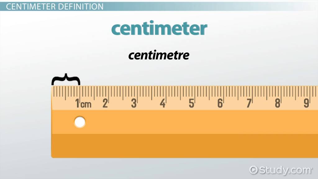
The Physicality of Tech: Why 1 Centimeter is the New Mile
In the early days of computing, hardware was measured in meters and feet. Mainframe computers occupied entire rooms. Today, the competitive edge of a consumer tech product is often determined by a single centimeter of thickness or the lack thereof.
The Evolution of the “Thin-and-Light” Category
If we look at the history of the laptop, the journey toward the sub-centimeter mark has been the primary driver of innovation. In the early 2000s, a “thin” laptop was three centimeters thick. When Steve Jobs pulled the original MacBook Air out of a manila envelope in 2008, the world was shocked by its 1.94 cm profile. Today, top-tier tablets and ultrabooks are pushing the boundaries of 0.5 cm to 1 cm.
When a manufacturer manages to shave off just one centimeter from a device’s chassis, it isn’t just an aesthetic choice. It represents a total reimagining of thermal management, battery density, and structural integrity. A device that is 1 cm thick requires specialized materials like CNC-machined aluminum or carbon fiber to ensure it doesn’t bend under the pressure of daily use.
The Impact on Hardware Internal Layout
Inside a modern smartphone, a space of 1 cm is enormous. To an engineer, 1 cm of unused space is a luxury that doesn’t exist. Components like the Taptic Engine, the camera module, and the logic board are fighting for fractions of millimeters. When we visualize 1 cm in this context, we are looking at the space required to house a high-resolution periscope zoom lens or a significant portion of a 5,000 mAh battery. Every centimeter gained through miniaturization is immediately reinvested into better sensors or longer battery life.
Micro-Engineering and the Scale of Modern Circuitry
To truly understand what 1 centimeter looks like in tech, one must look beneath the surface at the silicon level. This is where the scale of “one centimeter” becomes truly mind-boggling.
The Transistor Density Paradox
A modern high-end processor, such as Apple’s M-series or NVIDIA’s latest GPUs, often has a die size (the actual silicon chip) that is roughly 1 to 2 square centimeters. Within that 1 cm x 1 cm area, engineers are now able to fit upwards of 10 to 20 billion transistors.
When you look at a 1 cm square of silicon, you aren’t just looking at a piece of metal; you are looking at a “metropolis” of interconnected pathways. If you were to scale a single transistor up to the size of a human, that 1 cm chip would be the size of a massive city. The precision required to print these circuits at the 3-nanometer (nm) node means that 1 centimeter is now the host to a level of complexity that was once unthinkable.
The Challenges of Signal Integrity
At the scale of a few centimeters, electricity doesn’t just flow; it encounters resistance, heat, and interference. As chips get smaller and more powerful, the 1 cm distance between the CPU and the RAM becomes a bottleneck. This is why we are seeing a shift toward “System on a Chip” (SoC) designs and stacked memory. By reducing the physical distance that data must travel—moving it from 5 cm away to less than 1 cm away—manufacturers can significantly increase processing speed and reduce power consumption.

User Experience: How 1 Centimeter Changes Human-Computer Interaction
While engineers care about 1 cm in terms of circuitry, designers care about 1 cm in terms of the human body. The physical dimensions of our technology must interface with the biological dimensions of our hands, fingers, and eyes.
The “Golden Rule” of Touch Targets
In UI/UX (User Interface/User Experience) design, 1 centimeter is a critical threshold. The average human fingertip is about 8 to 10 millimeters wide. Therefore, for a digital button on a touchscreen to be “tappable” without error, it generally needs to be at least 1 cm wide.
If a developer reduces a button’s size to 0.5 cm, the “fat finger” effect takes over, leading to user frustration and accidental clicks. When you look at your smartphone screen, the layout is essentially a grid of 1 cm zones optimized for human dexterity. The visual design may be digital, but it is strictly governed by the physical reality of the centimeter.
Bezels and the “All-Screen” Illusion
For years, the goal of smartphone manufacturers was the “death of the bezel.” A bezel is the border between the screen and the frame of the device. Reducing the bezel by just 1 centimeter transformed the industry, allowing for larger displays without making the phones themselves too large to hold. This 1 cm difference is what separated the era of the iPhone 8 from the era of the iPhone 15. It represents the transition from a device with “forehead and chin” borders to an immersive, edge-to-edge experience.
The Future of Wearables: Shrinking 1 Centimeter into 1 Millimeter
As we move toward the next generation of gadgets—specifically augmented reality (AR) glasses and health-monitoring wearables—the centimeter is becoming the “final frontier” of bulk.
The Ergonomics of AR and VR
The primary hurdle for AR glasses is currently weight and volume. Most current prototypes are “bulky” because they protrude 2 or 3 centimeters from the face. For AR to become mainstream, the optics and batteries must be compressed into a form factor that is less than 1 cm thick. What does 1 cm look like here? It looks like the difference between a heavy headset that causes neck strain and a pair of sleek glasses that you can wear all day.
Bio-Sensing and Medical Tech
In the world of medical tech and fitness trackers, 1 centimeter is the difference between a bulky strap and a “smart skin” patch. Engineers are working to integrate sensors that can measure glucose levels, heart rate, and oxygen saturation within modules that are less than 1 cm in diameter. At this scale, the technology becomes “invisible.” The goal is to move past the centimeter and into the millimeter, where the device is no longer a “gadget” but a seamless extension of the human body.
Connectivity and the IoT
The Internet of Things (IoT) relies on small, low-power sensors placed in everything from lightbulbs to industrial machinery. A sensor that is 10 cm wide is a nuisance; a sensor that is 1 cm wide can be embedded anywhere. This miniaturization allows for a “connected world” where data is gathered from the smallest crevices of our environment.

Conclusion: The Magnitude of the Small
What does 1 centimeter look like? In the tech industry, it looks like a decade of progress. It is the thickness of a high-performance laptop, the width of a billion-transistor processor, and the ideal size for a touch-screen icon.
We often celebrate the “big” things in tech—massive data centers, giant satellite constellations, and 100-inch televisions. But the true mastery of modern technology lies in the “small.” The ability to manipulate matter at the centimeter level—and far below it—is what has allowed us to put the power of a 1990s supercomputer into a device that fits in a pocket.
As we look toward the future, the challenge for the tech world will be to continue doing more with less. We will continue to ask what 1 centimeter can hold, how much power it can generate, and how much data it can transmit. In the digital age, the centimeter is not just a unit of length; it is the ultimate measure of our ingenuity.
aViewFromTheCave is a participant in the Amazon Services LLC Associates Program, an affiliate advertising program designed to provide a means for sites to earn advertising fees by advertising and linking to Amazon.com. Amazon, the Amazon logo, AmazonSupply, and the AmazonSupply logo are trademarks of Amazon.com, Inc. or its affiliates. As an Amazon Associate we earn affiliate commissions from qualifying purchases.