
In the vast landscape of digital electronics, every action we perform—from sending a text message to rendering a complex 3D video game—is the result of millions of tiny switches operating at incredible speeds. At the heart of this binary world lies the logic gate. While there are several types of logic gates, such as AND, OR, and NOT, one stands above the rest in terms of utility and manufacturing importance: the NAND gate.
Often referred to as the “universal gate,” the NAND gate is the fundamental building block of modern computing architecture. Its ability to replicate the function of any other logic gate makes it the cornerstone of integrated circuits, microprocessors, and memory storage. Understanding the NAND gate is not just an exercise in electrical engineering; it is an exploration into the very language of the digital age.

Defining the NAND Gate: Logic, Symbols, and Functionality
The term “NAND” is a contraction of “NOT AND.” To understand its function, one must first understand the standard AND gate. In digital logic, an AND gate produces a “High” output (1) only when all of its inputs are “High.” If any input is “Low” (0), the output is Low. The NAND gate essentially takes this result and inverts it using a NOT operation.
The Logic of the NAND Operation
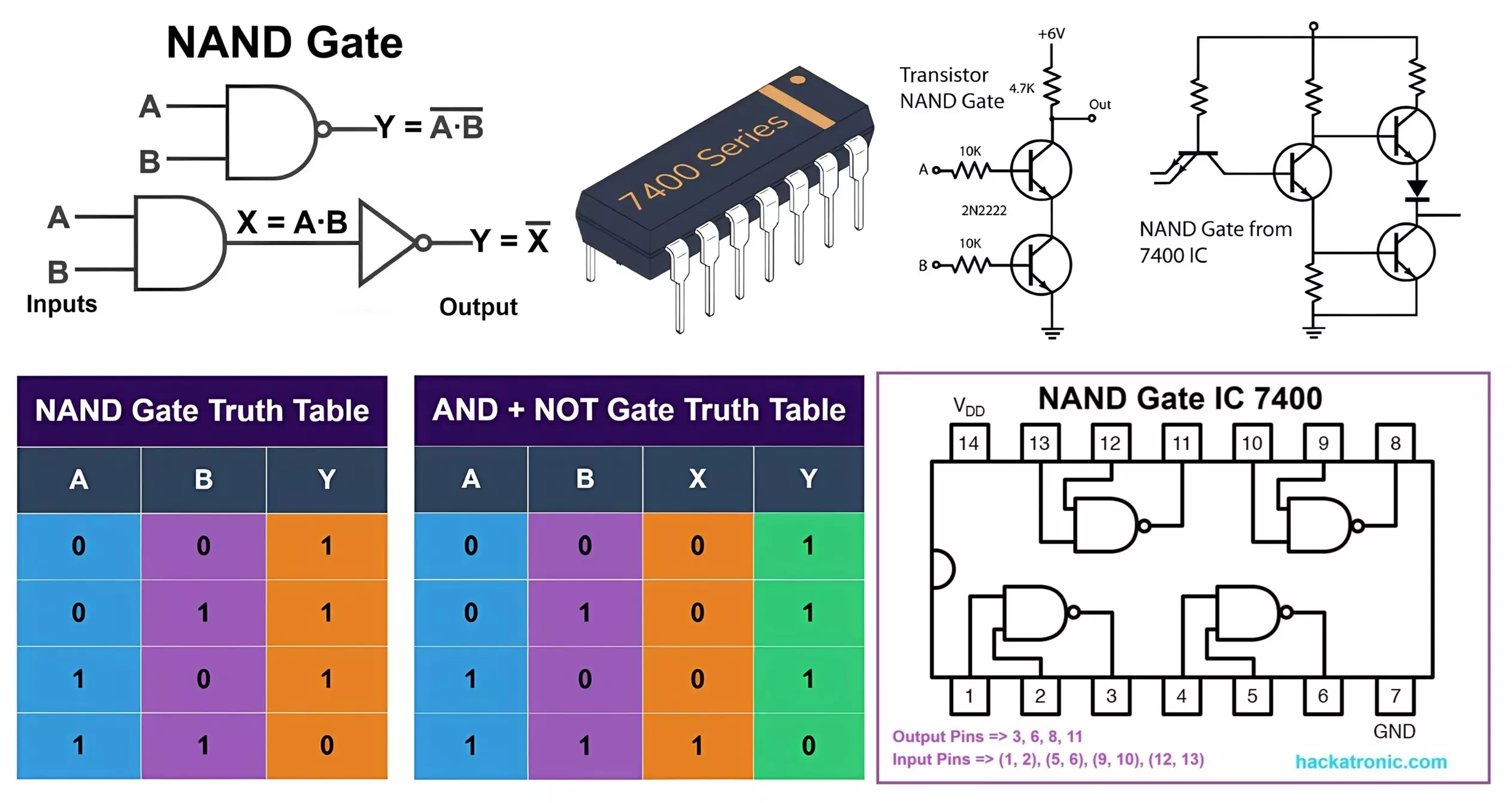
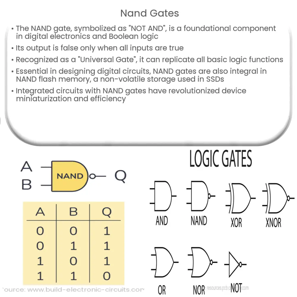
In simple terms, a NAND gate produces a “High” output at all times except when all of its inputs are “High.” If you provide two inputs, A and B, to a NAND gate, the output will be 0 only if both A and B are 1. In every other scenario—whether both are 0 or one is 1 and the other is 0—the output will be 1.
This “negative-AND” logic is represented mathematically through Boolean algebra. The Boolean expression for a NAND gate is written as $Y = overline{A cdot B}$. Here, the dot represents the AND operation, and the overline represents the inversion (NOT).
The Truth Table
To visualize how a NAND gate operates, engineers use a truth table. For a standard two-input NAND gate, the table is as follows:
- Input A: 0, Input B: 0 | Output: 1
- Input A: 0, Input B: 1 | Output: 1
- Input A: 1, Input B: 0 | Output: 1
- Input A: 1, Input B: 1 | Output: 0
Symbolic Representation
In circuit diagrams, the NAND gate is represented by a specific symbol: a “D” shape (the AND gate symbol) with a small circle, known as an inversion bubble, at the output tip. This bubble is the graphical representation of the NOT function, signaling to the engineer that the preceding logic is being flipped.
The “Universal Gate” Phenomenon: Why NAND Dominates Hardware
The NAND gate is mathematically categorized as a “universal gate.” This is a significant distinction in the world of computer science and hardware design. Functional completeness means that any boolean function can be implemented using only NAND gates.
Constructing Other Gates from NAND
Because the NAND gate is universal, a computer could, in theory, be built entirely out of NAND gates and nothing else.
- Creating a NOT gate: If you tie the two inputs of a NAND gate together, they will always receive the same signal. If the input is 1, the output is 0; if the input is 0, the output is 1. Thus, a NAND gate becomes a NOT gate.
- Creating an AND gate: By taking the output of a NAND gate and running it through a NOT gate (which we already know can be made from a NAND gate), the double inversion results in a standard AND operation.
- Creating an OR gate: According to De Morgan’s Laws, the inverse of a NAND gate with inverted inputs results in an OR operation. By inverting the inputs A and B individually (using NAND-based NOT gates) and then passing them through another NAND gate, you achieve the logic of an OR gate.
Economic and Manufacturing Efficiency
From a manufacturing perspective, using a single type of gate to build complex processors is highly efficient. When a fabrication plant (a “fab”) produces silicon wafers, it is easier and more cost-effective to optimize the production of one specific transistor arrangement. By designing circuits that primarily utilize NAND logic, manufacturers can achieve higher transistor density, lower power consumption, and reduced production costs. This is one of the primary reasons why NAND architecture is so prevalent in modern microchips.
NAND in Practice: The Evolution of NAND Flash Memory
While “NAND” refers to a logic gate, most people encounter the term today in the context of “NAND Flash Memory.” This is the non-volatile storage technology found in Solid State Drives (SSDs), USB thumb drives, and smartphones. While the logic gate and the memory cell are different physical implementations, the underlying “Not-AND” architecture is what gives this storage its name.
How NAND Flash Works
NAND flash memory stores data in an array of memory cells made from floating-gate transistors. Unlike traditional RAM, which loses its data when power is disconnected, NAND flash retains its state. It organizes these cells in a way that resembles the NAND logic gate’s serial wiring, allowing for high-density storage.
The Advantage of NAND over NOR
In the early days of flash memory, there were two competing architectures: NAND and NOR.
- NOR Flash allows for fast random access, making it ideal for storing the code that boots up a computer (BIOS). However, it is physically larger and more expensive to produce.
- NAND Flash has slower random access but offers much higher storage density and faster “write” and “erase” speeds. Because of its serial-like structure, it requires less space on the silicon, which is why we can now fit terabytes of data into a device the size of a postage stamp.
SLC, MLC, and TLC Architectures
As technology has progressed, engineers have found ways to squeeze more data into NAND cells.
- Single-Level Cell (SLC): Stores one bit per cell. It is the fastest and most durable but the most expensive.
- Multi-Level Cell (MLC): Stores two bits per cell.
- Triple-Level Cell (TLC): Stores three bits per cell. This is what most consumer-grade SSDs use today, balancing cost and performance.
The Physical Architecture: Transistors and CMOS Technology
To truly understand a NAND gate, one must look at how it is physically constructed at the microscopic level. In modern electronics, this is achieved using Complementary Metal-Oxide-Semiconductor (CMOS) technology.
PMOS and NMOS Transistors
A CMOS NAND gate is built using two types of transistors: P-type (PMOS) and N-type (NMOS).
- In a NAND configuration, the PMOS transistors are connected in parallel to the power source.
- The NMOS transistors are connected in series to the ground.
When both inputs are “High” (1), the NMOS path to the ground is completed, and the PMOS path to the power source is cut off, resulting in a “Low” (0) output. If either input is “Low” (0), at least one PMOS transistor allows current to flow from the power source to the output, while the NMOS path to the ground is broken, resulting in a “High” (1) output.
Miniaturization and Moore’s Law
For decades, the tech industry followed Moore’s Law, which predicted that the number of transistors on a chip would double approximately every two years. As NAND gates have shrunk to the nanometer scale (with current processes reaching 3nm and beyond), engineers face significant challenges such as quantum tunneling and heat dissipation. Despite these hurdles, the NAND gate remains the most scalable architecture for continuing the trend of increasing computational power.
The Future of Logic Gates: AI and Beyond
As we move into the era of Artificial Intelligence and Quantum Computing, the role of the traditional NAND gate is evolving. While binary logic remains the standard, new hardware paradigms are emerging to handle the massive datasets required by modern AI.
Neuromorphic Computing and AI Accelerators
Traditional CPUs use a “Von Neumann architecture” where logic (NAND gates) and memory are separate. This creates a bottleneck when processing AI workloads. New “AI chips” or Neural Processing Units (NPUs) are being designed to mimic the human brain’s structure, integrating logic and memory more closely. Even in these advanced architectures, the fundamental principles of Boolean logic—pioneered by the NAND gate—remain the theoretical foundation.
Quantum Logic Gates
Quantum computing introduces the “Qubit,” which can exist in multiple states simultaneously. Quantum logic gates (like the Hadamard gate or the CNOT gate) operate on entirely different physical principles than the silicon NAND gate. However, for the foreseeable future, quantum computers will act as specialized co-processors to classical silicon-based systems. The NAND gate will continue to manage the interface, the storage, and the primary logic of the machines that run our world.
Conclusion
The NAND gate is a testament to the power of simplicity. From a single mathematical concept—inverting an AND operation—humanity has built a digital civilization. It is the “universal” nature of this gate that allowed for the mass production of affordable, powerful electronics. Whether it is acting as a logical switch in a processor or a storage cell in an SSD, the NAND gate is the silent engine of the information age. As we push toward the limits of physics in semiconductor manufacturing, the legacy of the NAND gate as the ultimate building block of technology remains undisputed.
aViewFromTheCave is a participant in the Amazon Services LLC Associates Program, an affiliate advertising program designed to provide a means for sites to earn advertising fees by advertising and linking to Amazon.com. Amazon, the Amazon logo, AmazonSupply, and the AmazonSupply logo are trademarks of Amazon.com, Inc. or its affiliates. As an Amazon Associate we earn affiliate commissions from qualifying purchases.