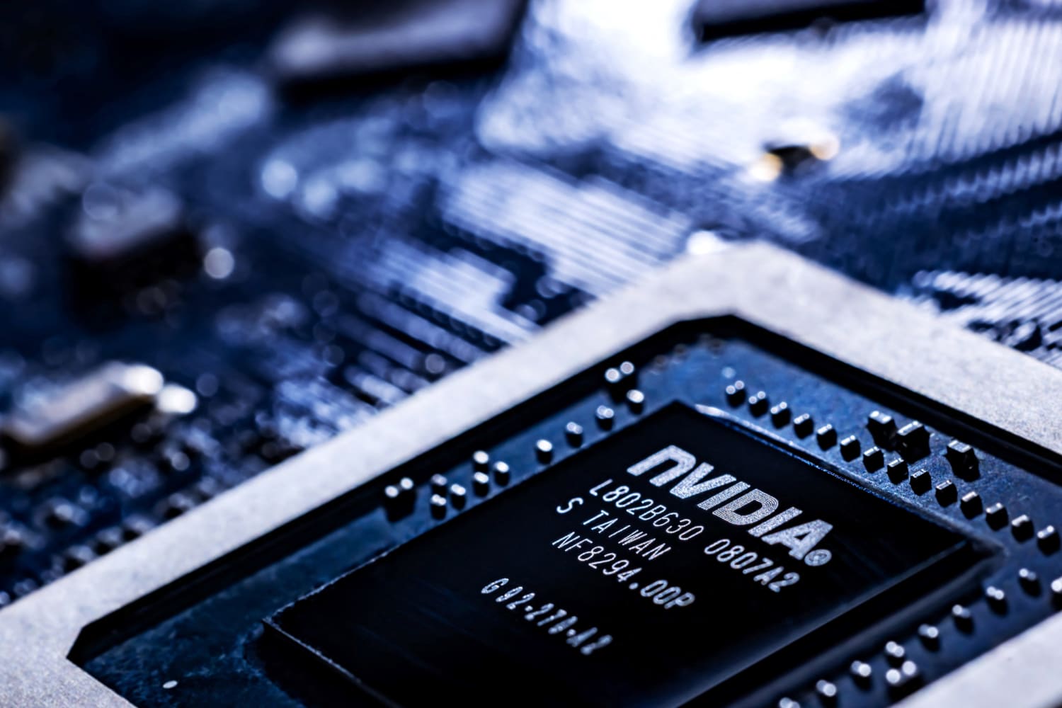
The name Nvidia is synonymous with cutting-edge graphics processing units (GPUs), artificial intelligence (AI) acceleration, and high-performance computing. From powering the most demanding PC games to enabling breakthroughs in scientific research and autonomous vehicles, Nvidia’s silicon is at the heart of countless technological advancements. A seemingly straightforward question — “where does Nvidia make their chips?” — unearths a fascinating and incredibly complex global supply chain, revealing a sophisticated ecosystem of design, manufacturing, and assembly that defines the modern semiconductor industry.
Unlike traditional Integrated Device Manufacturers (IDMs) like Intel, which historically designed and fabricated their own chips, Nvidia operates on a “fabless” model. This strategic choice places Nvidia at the forefront of chip design and innovation, leveraging the specialized capabilities of dedicated third-party foundries for physical production. The result is a highly efficient, globally distributed network where Nvidia’s brilliant architectural designs are transformed into tangible silicon, primarily within the advanced facilities of Taiwan Semiconductor Manufacturing Company (TSMC), and occasionally others like Samsung Foundry.
The “Fabless” Model: Nvidia’s Strategic Choice
Nvidia’s success is deeply intertwined with its adoption of the fabless business model, a strategic decision that has allowed the company to channel its resources into core competencies while offloading the immense capital expenditure and operational complexities associated with semiconductor manufacturing. This model is not just a preference; it’s a fundamental pillar of its technological dominance.
Understanding Fabless Semiconductor Companies
A “fabless” semiconductor company, as the name suggests, designs and markets integrated circuits but does not own or operate a semiconductor fabrication plant (a “fab”). Instead, these companies outsource the actual manufacturing of their silicon wafers to specialized third-party foundries. This contrasts sharply with the “Integrated Device Manufacturer” (IDM) model, where a single company handles everything from design to fabrication, assembly, and testing. Intel, for a significant part of its history, exemplified the IDM model, investing billions in its own state-of-the-art fabs.
For fabless companies like Nvidia, the primary focus is on research and development (R&D), chip architecture, logic design, software development (like CUDA for GPUs), and market positioning. This specialization allows them to attract top talent in chip design, cultivate deep expertise in specific application areas, and remain agile in a rapidly evolving technological landscape. The intellectual property (IP) and design methodologies are their crown jewels, not the physical machinery of production.
Why Fabless Works for Nvidia
The fabless model offers compelling advantages that have been crucial for Nvidia’s ascent to its current market position:
- Focus on Core Competencies: By not owning fabs, Nvidia can dedicate virtually all its engineering and financial resources to GPU architecture, AI algorithms, software ecosystems, and innovative chip designs. This intense focus drives the breakthroughs that distinguish its products.
- Access to Cutting-Edge Process Nodes: Semiconductor manufacturing requires astronomical capital investments. Each new process node (e.g., moving from 7nm to 5nm or 3nm) demands billions of dollars in new equipment and R&D. By partnering with leading foundries, Nvidia gains immediate access to the most advanced manufacturing technologies without incurring these prohibitive costs. This enables them to rapidly integrate the latest transistor densities and performance improvements into their designs.
- Flexibility and Scalability: Foundries offer a flexible manufacturing capacity that fabless companies can tap into based on market demand. This allows Nvidia to scale production up or down more easily than if it had to manage its own fixed-capacity fabs. It also reduces financial risk associated with potential underutilization of expensive manufacturing facilities during market downturns.
- Reduced Financial Risk: The semiconductor industry is cyclical and highly capital-intensive. Owning and maintaining fabs exposes a company to massive depreciation, technological obsolescence risk, and the burden of continuous upgrades. The fabless model insulates Nvidia from these direct manufacturing-related financial pressures, allowing for more stable financial performance and greater investment in innovation.
The Architects of Silicon: Key Foundry Partners
While Nvidia designs the intricate blueprints for its powerful processors, it is the highly specialized foundries that possess the expertise, technology, and infrastructure to bring these designs to life. In this critical partnership, a few players stand out as indispensable to Nvidia’s production strategy.
TSMC: The Undisputed Kingpin
Taiwan Semiconductor Manufacturing Company (TSMC) is, without question, Nvidia’s most crucial and primary manufacturing partner. Often referred to as the “foundry to the world,” TSMC is a titan in semiconductor manufacturing, renowned for its technological leadership, massive scale, and impeccable reputation for quality and innovation.
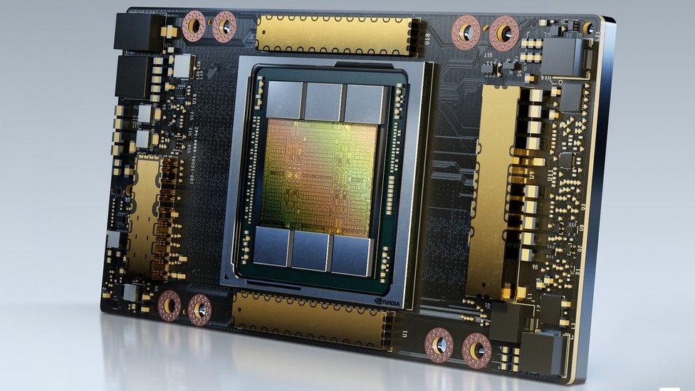
Nvidia relies heavily on TSMC for fabricating its most advanced and highest-performance GPUs, including the latest generations of its GeForce consumer graphics cards, professional Quadro GPUs, and, most critically, its high-end data center and AI accelerators (like the Hopper and Blackwell architectures). TSMC’s consistent leadership in developing and perfecting cutting-edge process nodes (such as 7nm, 5nm, 4nm, and the upcoming 3nm and 2nm technologies) is fundamental to Nvidia’s ability to pack billions of transistors into its chips, enabling unprecedented levels of performance and energy efficiency. The sophisticated manufacturing processes required for these advanced nodes demand extreme precision, ultra-clean environments, and multi-billion-dollar equipment, particularly from companies like ASML for lithography, capabilities that only a handful of foundries globally possess, with TSMC at the forefront.
Samsung Foundry: A Secondary but Growing Player
While TSMC handles the bulk of Nvidia’s bleeding-edge production, Samsung Foundry has also played a significant role, particularly in specific product generations or to diversify Nvidia’s supply chain. For instance, parts of the Nvidia Ampere generation (e.g., the RTX 30 series consumer GPUs) utilized Samsung’s 8nm process node for some of its product stack.
Samsung Foundry, part of the larger Samsung Group, is a major competitor to TSMC, investing heavily to catch up and offer compelling alternatives. Using multiple foundries offers several advantages to Nvidia: it provides supply chain resilience by reducing sole reliance on a single vendor, potentially introduces competitive pricing dynamics, and allows access to specialized process nodes that might be better suited for certain products or cost targets. Samsung’s expertise, particularly in memory technologies and advanced packaging, also makes it an attractive partner for certain integrated chip designs.
The Role of Other Foundries
While TSMC and Samsung are paramount for Nvidia’s high-performance products, other foundries exist within the broader semiconductor landscape. Companies like UMC (United Microelectronics Corporation) and GlobalFoundries are significant players, though they typically specialize in less bleeding-edge or more mature process nodes. These foundries might be utilized by Nvidia for older or more specialized chips (e.g., embedded processors, display controllers, or older generations of GPUs that don’t require the absolute latest technology). Their role for Nvidia’s flagship products is limited, but they remain vital components of the global chip ecosystem, manufacturing a vast array of semiconductors for numerous applications.
The Global Tapestry of Chip Production: Beyond the Foundry
Understanding “where” Nvidia’s chips are made extends beyond identifying the foundry. It encompasses a complex, multi-stage process involving numerous specialized companies across the globe, each contributing a vital piece to the final product.
Design and IP Cores
The journey begins long before a wafer enters a fab. Nvidia’s brilliant engineers design the intricate architecture of its GPUs, including the famous CUDA cores, Tensor Cores for AI acceleration, and RT Cores for real-time ray tracing. This involves extensive simulation, verification, and optimization. Furthermore, Nvidia often integrates “Intellectual Property” (IP) cores from third-party vendors for standard functions like ARM cores for embedded controllers within the GPU, or various interface controllers (PCIe, DisplayPort, HDMI). This collaborative design approach, facilitated by Electronic Design Automation (EDA) tools, allows Nvidia to build incredibly complex systems-on-a-chip (SoCs) efficiently.
Frontend Manufacturing (Wafer Fabrication)
This is the core function of the foundries like TSMC and Samsung. Frontend manufacturing involves taking raw, ultra-pure silicon wafers and building the foundational electronic circuits on them. This process is astonishingly complex and precise, often involving hundreds of steps:
- Deposition: Applying thin films of various materials (conductors, insulators, semiconductors).
- Lithography: Using light (including extreme ultraviolet or EUV for advanced nodes) to pattern these layers, defining the billions of transistors and interconnections.
- Etching: Removing unwanted material, leaving behind the patterned structures.
- Doping: Introducing impurities to silicon to create p-type and n-type semiconductor regions, forming transistors.
- Chemical Mechanical Planarization (CMP): Polishing surfaces to ensure flatness for subsequent layers.
This entire process occurs in ultra-cleanroom environments, typically 10,000 times cleaner than a hospital operating room, to prevent microscopic dust particles from ruining the delicate circuits.
Backend Manufacturing (Assembly, Testing, Packaging)
Once the wafers are fabricated at the foundry, they embark on the final stages of their journey, often handled by specialized outsourced semiconductor assembly and test (OSAT) companies, frequently located in Southeast Asia (e.g., Malaysia, Taiwan, China):
- Wafer Dicing: The large circular silicon wafer is cut into hundreds or thousands of individual rectangular “dies” (the actual chips).
- Die Bonding: Each good die is then mounted onto a substrate, which provides electrical and mechanical connections.
- Wire Bonding/Flip-Chip: Tiny gold wires are used to connect the die to the package leads, or in more advanced packaging, the die is “flipped” directly onto the substrate with solder bumps.
- Packaging: The assembled die and substrate are encapsulated in a protective package (e.g., Ball Grid Array – BGA, Multi-Chip Module – MCM) that protects the delicate chip and allows it to be soldered onto a circuit board. Advanced packaging, like integrating High Bandwidth Memory (HBM) alongside the GPU die on an interposer, is crucial for high-performance data center accelerators.
- Testing: Rigorous testing is performed at various stages – at the wafer level, after packaging, and sometimes at the system level – to ensure functionality, performance, and reliability. This identifies defective chips and ensures only high-quality products reach the market.
Navigating the Complexities and Future of Semiconductor Manufacturing
The intricate global supply chain for semiconductors, while enabling unparalleled technological advancement, also presents significant challenges and strategic considerations for companies like Nvidia and governments worldwide.
Supply Chain Vulnerabilities and Geopolitical Considerations
The concentration of advanced semiconductor manufacturing capabilities, particularly in Taiwan with TSMC, has become a major geopolitical concern. The COVID-19 pandemic vividly exposed the fragility of global supply chains, leading to widespread chip shortages that impacted numerous industries. This dependence on a single region for cutting-edge fabrication creates strategic vulnerabilities.
In response, governments in the United States (with the CHIPS and Science Act), Europe (EU Chips Act), and other regions are initiating multi-billion-dollar efforts to incentivize and subsidize the localization and diversification of semiconductor manufacturing. While Nvidia will likely continue its primary partnership with TSMC, it also benefits from and contributes to efforts that build more resilient and geographically dispersed manufacturing capabilities, ensuring a stable supply for its diverse product portfolio.
The Drive for Innovation and Cost Efficiency
Moore’s Law, the observation that the number of transistors on a microchip doubles roughly every two years, has been a driving force for decades. However, the physical and economic challenges of shrinking process nodes are becoming increasingly daunting. The cost of designing and manufacturing at 3nm or 2nm is astronomical.
This has led to new avenues of innovation beyond simple transistor scaling. Advanced packaging techniques, such as chiplets (where different functional blocks are manufactured on separate dies and then integrated into a single package) and 3D stacking (layering dies vertically), are becoming critical for achieving higher performance, improved power efficiency, and better yields. Nvidia is at the forefront of adopting these techniques, enabling the creation of powerful GPUs that overcome the limitations of traditional monolithic designs. The continuous race involves not just smaller transistors, but smarter ways to integrate and interconnect them.
Environmental Impact and Sustainability
The semiconductor manufacturing process is notoriously resource-intensive, consuming significant amounts of energy, ultra-pure water, and various chemicals. As global awareness of environmental issues grows, the industry faces increasing pressure to adopt more sustainable practices. Foundries and fabless companies are investing in greener manufacturing processes, reducing waste, optimizing energy consumption, and exploring renewable energy sources. Nvidia, as a major consumer of foundry services, indirectly influences these trends by partnering with foundries that demonstrate a commitment to environmental stewardship.

Conclusion
Nvidia does not “make” its chips in its own factories in the traditional sense. Instead, it operates as a sophisticated fabless semiconductor company, a master architect of silicon that meticulously designs its groundbreaking GPUs and AI processors. The actual fabrication of these complex designs is then entrusted to a select group of highly advanced third-party foundries, predominantly TSMC, with Samsung Foundry playing a supporting role.
This distributed, specialized ecosystem highlights the intricate global collaboration that underpins modern technology. Nvidia’s strength lies in its unparalleled design innovation, while its manufacturing partners provide the cutting-edge process technology required to turn those designs into reality. The future of where Nvidia’s chips are made will likely continue to revolve around these advanced foundries, but with an increasing emphasis on diversifying supply chains, leveraging advanced packaging, and navigating geopolitical shifts, all while relentlessly pushing the boundaries of what silicon can achieve. The interplay between ingenious design and manufacturing prowess remains the cornerstone of Nvidia’s continued dominance in the tech world.
aViewFromTheCave is a participant in the Amazon Services LLC Associates Program, an affiliate advertising program designed to provide a means for sites to earn advertising fees by advertising and linking to Amazon.com. Amazon, the Amazon logo, AmazonSupply, and the AmazonSupply logo are trademarks of Amazon.com, Inc. or its affiliates. As an Amazon Associate we earn affiliate commissions from qualifying purchases.