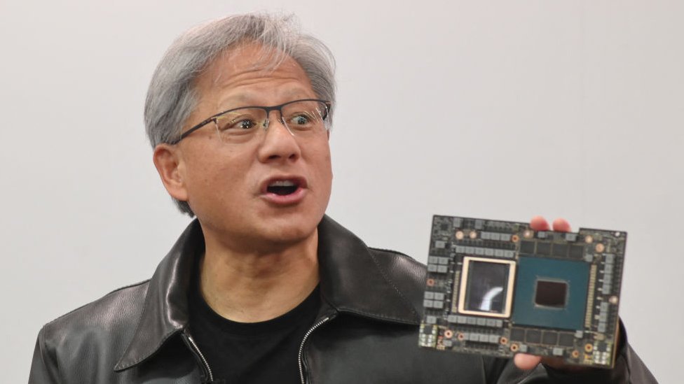
In the intricate world of high technology, few names command as much respect and influence as Nvidia. From powering cutting-edge gaming experiences to accelerating the most complex AI research and data center operations, Nvidia’s Graphics Processing Units (GPUs) have become indispensable. Given their ubiquitous presence and critical role, a fundamental question often arises: “Who actually makes Nvidia chips?” The answer, while seemingly straightforward, unravels a fascinating and incredibly complex global ecosystem that defines the modern semiconductor industry. Far from being a vertically integrated manufacturing giant, Nvidia operates on a “fabless” model, designing its revolutionary chips while entrusting their physical creation to a select few, highly specialized manufacturing partners.
The Fabless Business Model: Nvidia’s Core Strategy
Nvidia’s ascent to its current stature is intrinsically linked to its strategic adoption of the fabless semiconductor model. This approach allows the company to focus its formidable resources and intellectual capital on what it does best: pioneering chip architecture and innovative software platforms, rather than the gargantuan capital expenditures and operational complexities of owning and running semiconductor fabrication plants (fabs).
Designing the Future: Nvidia’s Intellectual Property
At its heart, Nvidia is a design house. Its core competency lies in the research and development of highly complex chip architectures, primarily its acclaimed GPUs, but also including system-on-chips (SoCs) and networking solutions. This involves an army of engineers and scientists dedicated to microarchitecture, logic design, circuit design, and the development of supporting software ecosystems like CUDA, which unlocks the parallel processing power of its GPUs for a vast array of scientific and computational tasks.
Nvidia’s intellectual property (IP) is its most valuable asset. Each new generation of GPUs, such as the Hopper or Ada Lovelace architectures, represents years of intensive R&D, pushing the boundaries of transistor density, power efficiency, and computational capability. The company meticulously crafts every aspect of the chip’s blueprint, from the individual processing cores to the memory interfaces and interconnects. This includes defining the exact specifications, performance targets, and even collaborating on the process technology requirements with its manufacturing partners to ensure the designs can be brought to life effectively. This relentless pursuit of design innovation is what keeps Nvidia at the forefront of AI, high-performance computing, and gaming.
The Rationale Behind Going Fabless
The decision to remain fabless is not arbitrary; it’s a strategic imperative driven by the economics and technological realities of the semiconductor industry. Building and maintaining a leading-edge semiconductor fab is an undertaking of colossal scale and cost, often running into tens of billions of dollars for a single facility. These fabs require highly specialized cleanroom environments, an incredible array of precision equipment (some costing hundreds of millions apiece), and an army of highly skilled technicians and engineers.
By operating fabless, Nvidia avoids these astronomical capital expenditures, allowing it to reallocate those funds into R&D, talent acquisition, and market expansion. This specialization fosters efficiency: Nvidia focuses solely on design, while its foundry partners specialize solely on manufacturing. This division of labor allows each entity to achieve world-class excellence in its respective domain. Furthermore, the fabless model offers tremendous flexibility and scalability. Nvidia can adapt to market shifts more nimbly, leveraging the production capacity of multiple foundries if needed, without being burdened by the fixed costs and operational overhead of its own manufacturing plants. It also mitigates significant financial and operational risks associated with a capital-intensive industry known for its brutal cycles of boom and bust.
The Titans of Fabrication: TSMC and Samsung Foundry
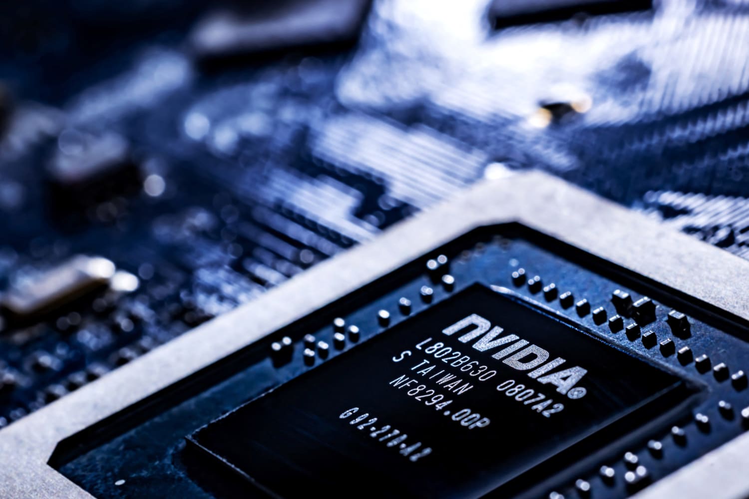
While Nvidia designs the masterpieces, it is the sophisticated foundries that meticulously etch these designs onto silicon wafers. In this crucial role, two companies stand out as the primary manufacturing partners for Nvidia’s most advanced chips: Taiwan Semiconductor Manufacturing Company (TSMC) and, to a lesser extent, Samsung Foundry.
TSMC: The Undisputed Leader
Taiwan Semiconductor Manufacturing Company (TSMC) is the unchallenged behemoth of the pure-play foundry market. A pure-play foundry means that TSMC does not design or sell its own chips; its sole business is to manufacture chips for other companies based on their designs. This business model has allowed TSMC to focus intensely on perfecting its manufacturing processes, leading to unparalleled expertise and technological leadership.
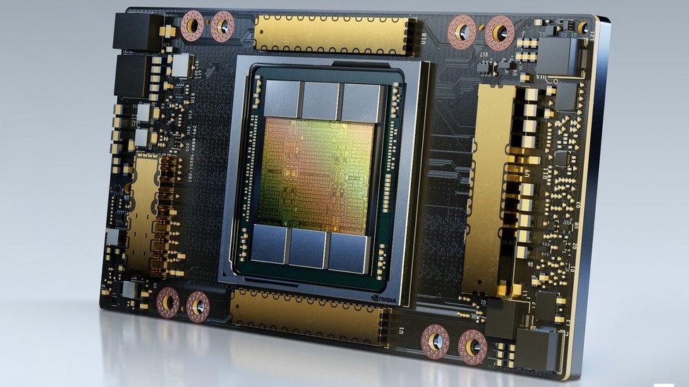
Nvidia has maintained a long-standing, critical partnership with TSMC. For its most advanced and highest-performing GPUs, particularly those destined for data centers, AI accelerators (like the H100 and GH200), and high-end gaming cards, Nvidia predominantly relies on TSMC’s cutting-edge process nodes. TSMC’s consistent ability to deliver the smallest, most efficient, and highest-yielding process technologies (e.g., 4nm, 3nm, and future nodes) is a cornerstone of Nvidia’s ability to innovate. These advanced nodes are crucial for packing billions of transistors onto a single chip, leading to significant gains in performance, power efficiency, and transistor density—all vital for the demanding workloads Nvidia’s chips are designed for. The geographical concentration of such advanced manufacturing in Taiwan, primarily with TSMC, also highlights a key geopolitical and supply chain consideration for the entire tech industry.
Samsung Foundry: A Growing Competitor
While TSMC handles the bulk of Nvidia’s leading-edge production, Samsung Foundry has also played a role in manufacturing some of Nvidia’s GPUs. Samsung is unique in the semiconductor landscape as an Integrated Device Manufacturer (IDM), meaning it designs, manufactures, and sells its own chips (e.g., Exynos processors for its phones, memory, storage). However, it also operates a dedicated foundry business, competing directly with TSMC for external clients.
Nvidia has engaged with Samsung Foundry for certain generations and product lines. For instance, a portion of the GeForce RTX 30 series (Ampere architecture) was manufactured on Samsung’s 8nm process node. This diversification of manufacturing partners can be a strategic move for Nvidia, potentially offering advantages in terms of supply chain resilience, cost negotiation, and access to different process technologies. Samsung Foundry is a formidable player, constantly investing heavily in R&D and manufacturing capabilities, including being at the forefront of implementing Gate-All-Around FET (GAAFET) technology, which represents the next major evolution in transistor design beyond FinFET. This technological rivalry between TSMC and Samsung pushes the boundaries of what’s possible in chip manufacturing, benefiting fabless companies like Nvidia.
Beyond the Foundry: The Intricate Semiconductor Supply Chain
The journey of an Nvidia chip doesn’t end at the foundry. The fabrication of the silicon wafer is just one, albeit critical, stage in a vast and highly specialized global supply chain. The complexity continues with raw materials, specialized equipment, and sophisticated post-fabrication processes.
Materials and Equipment: The Foundation of Chipmaking
Before a chip design can even be etched onto silicon, an entire ecosystem of specialized companies provides the foundational elements. High-purity silicon wafers, the literal canvases for microchips, come from companies like Shin-Etsu Chemical and SUMCO. Highly specialized chemicals, gases, and photoresists—light-sensitive materials crucial for photolithography—are supplied by a myriad of global leaders.
Equally vital are the manufacturers of the precision machinery used in fabs. Companies like ASML Holding N.V. are monopolistic suppliers of extreme ultraviolet (EUV) lithography machines, the most advanced tools for etching incredibly fine patterns onto wafers. Applied Materials, Lam Research, and KLA Corporation provide critical equipment for deposition, etching, inspection, and process control. Without this intricate web of highly specialized material and equipment providers, the concept of modern chip manufacturing, and by extension, Nvidia’s products, would simply not exist.
Packaging, Assembly, and Testing (OSAT)
Once silicon wafers emerge from the foundry with thousands of identical chips (dies), they are far from being finished products. These wafers are then sent to Outsourced Semiconductor Assembly and Test (OSAT) companies. Firms like ASE Technology Holding Co., Amkor Technology, and SPIL (Siliconware Precision Industries) perform the crucial final steps:
- Dicing: The wafer is cut into individual dies.
- Packaging: Each die is mounted onto a substrate, connected via tiny wires or solder bumps (wire bonding or flip-chip technology) to the package, which then provides electrical connections to the outside world and protects the delicate chip. This stage is increasingly complex, especially for high-performance chips that integrate multiple dies (e.g., GPU die with HBM memory stacks) using advanced packaging techniques like 2.5D or 3D integration.
- Testing: The packaged chips undergo rigorous electrical and functional testing to ensure they meet performance specifications and are free of defects. Only chips that pass these stringent tests are deemed ready for market.
These OSAT services are fundamental to ensuring the reliability, performance, and physical integrity of every Nvidia chip before it’s shipped to board partners or directly integrated into Nvidia’s own products.
The Strategic Implications and Future Outlook
The “who makes Nvidia chips” question, therefore, transcends a simple query about manufacturing. It reveals a landscape of profound strategic implications, shaping global economics, technological progress, and geopolitical dynamics.
Geopolitical Dynamics and Supply Chain Resilience
The high concentration of advanced semiconductor manufacturing in East Asia, particularly Taiwan with TSMC, presents both incredible efficiency and significant geopolitical risks. The reliance on a single region for critical components has prompted global efforts to diversify and localize chip production. Governments in the United States, Europe, and Japan are heavily subsidizing the construction of new fabs within their borders, aiming to enhance supply chain resilience and national security. Nvidia, like other fabless companies, actively monitors these developments and strategizes its manufacturing partnerships to navigate this evolving landscape, balancing cutting-edge technology access with geographical diversification. The ongoing “chip wars” and trade tensions underscore the strategic importance of semiconductor manufacturing and its role in global power dynamics.
The Race for Next-Gen Technologies
The demand for ever-more powerful, energy-efficient, and smaller chips is relentless, driven by the explosive growth of AI, autonomous vehicles, virtual reality, and cloud computing. This continuous demand fuels an intense race for next-generation technologies in both chip design and manufacturing. Nvidia’s ability to innovate in GPU architectures and software must be perfectly complemented by the foundries’ ability to shrink transistors further, develop new materials, and perfect novel packaging techniques.
Future innovations will likely include advancements in areas such as heterogeneous integration (combining different types of chips in a single package), photonics, quantum computing components, and entirely new transistor designs. Nvidia, through its close collaborations with TSMC, Samsung, and its extensive network of supply chain partners, is not just a consumer of these manufacturing advancements but an active participant in pushing their boundaries, ensuring that the innovations it designs can indeed be built for the future.
In conclusion, “who makes Nvidia chips” is a story of global collaboration, hyper-specialization, and technological mastery. Nvidia, the visionary architect, designs the future of computing. TSMC and Samsung, the master builders, bring these designs to life with unparalleled precision. And an intricate web of material suppliers, equipment manufacturers, and packaging specialists ensures that these marvels of engineering eventually reach the hands of consumers and enterprises worldwide. This distributed yet synchronized ecosystem is a testament to the complex, interdependent nature of the modern technology landscape, where innovation thrives on shared expertise across continents.
aViewFromTheCave is a participant in the Amazon Services LLC Associates Program, an affiliate advertising program designed to provide a means for sites to earn advertising fees by advertising and linking to Amazon.com. Amazon, the Amazon logo, AmazonSupply, and the AmazonSupply logo are trademarks of Amazon.com, Inc. or its affiliates. As an Amazon Associate we earn affiliate commissions from qualifying purchases.