
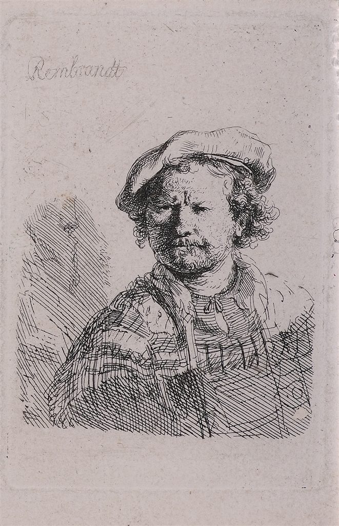
The term “etching” traditionally evokes images of Renaissance workshops, where master artists like Rembrandt painstakingly scratched intricate designs into copper plates to create timeless prints. However, in the modern landscape, the “art of etching” has undergone a radical technological transformation. No longer confined to the walls of a gallery, etching serves as the foundational process for the most complex machines ever built by humanity: the semiconductor chip.
In the tech industry, etching is the bridge between conceptual design and physical hardware. It is the method by which we translate the “art” of architectural circuit design onto silicon wafers. This article explores how etching has evolved from a 15th-century printmaking technique into a cornerstone of modern computing, digital security, and nanotech engineering.
The Technological Foundation: How Traditional Art Techniques Birthed Modern Computing
To understand the role of etching in technology, one must first recognize that the core principles have remained remarkably consistent for centuries. Traditional etching involves using a corrosive agent—typically an acid—to bite into the unprotected parts of a metal surface. In technology, we have simply refined the tools, moving from manual hand-tools to high-energy plasma and ultraviolet light.
The Intaglio Legacy: Precision in the Pre-Digital Era
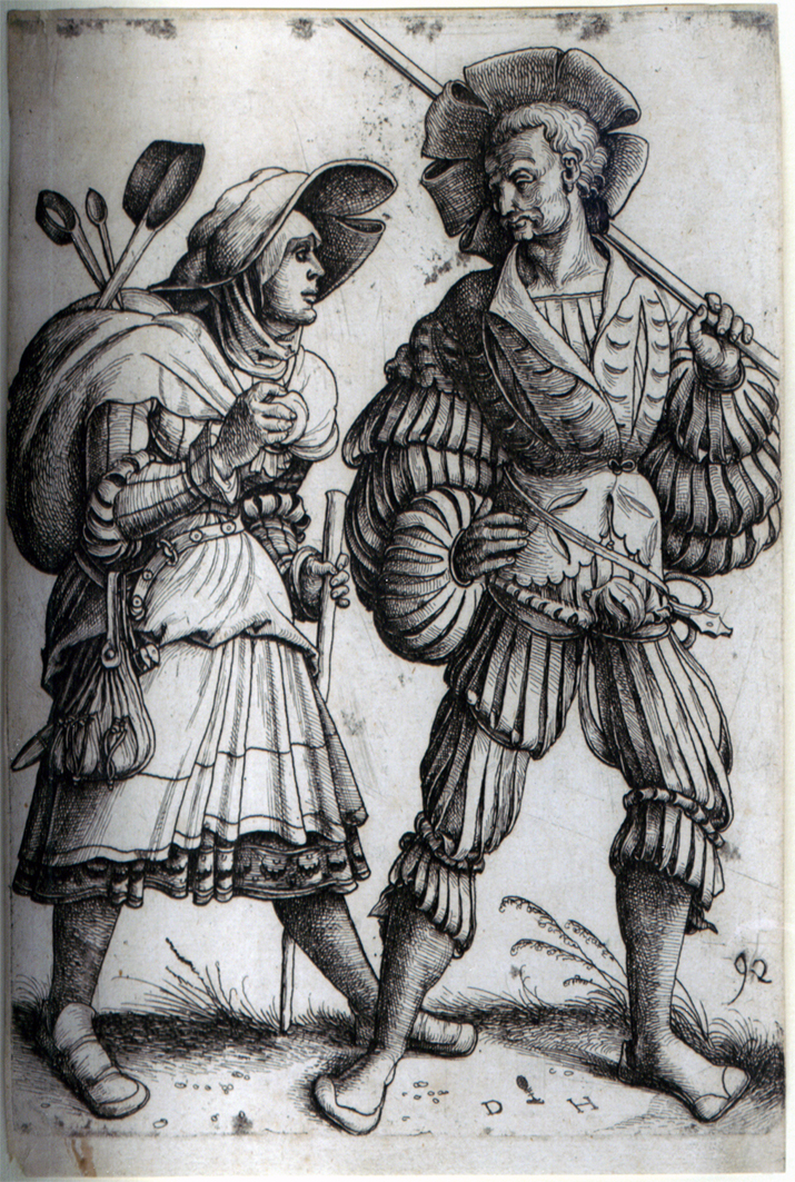
The “art” of etching began with the intaglio process. An artist would coat a metal plate with an acid-resistant wax or “ground.” By scratching through this ground, the artist exposed the metal. When the plate was submerged in acid, only the exposed lines were eaten away, creating a recessed image that could hold ink.
From a technological standpoint, this was the first instance of “masked” manufacturing. The wax acted as a primitive photoresist, a concept that remains the backbone of every microprocessor manufacturer today, from Intel to TSMC. The ability to achieve fine lines through chemical reactions rather than physical force allowed for a level of detail that traditional engraving could not match, paving the way for the micro-scale precision required in modern gadgets.
Transferred Knowledge: From Acid Baths to Chemical Vapor Deposition
As the industrial revolution transitioned into the digital revolution, the tech sector borrowed the chemistry of art to solve the problem of miniaturization. In the mid-20th century, engineers realized that if they could “etch” circuits instead of wiring them by hand, they could shrink the size of electronics exponentially.
This transition marked the birth of the printed circuit board (PCB) and, eventually, the integrated circuit. The “art” shifted from the aesthetic to the functional; instead of creating a landscape, engineers were “etching” logical pathways. The chemical baths were replaced by more controlled environments, but the fundamental logic remained: use a protective layer to define a pattern and use a reactive agent to remove the unwanted material.
Photolithography: The Master Art of Semiconductor Etching
If traditional etching is the grandfather of the tech world, photolithography is its most sophisticated descendant. In this context, “etching in art” refers to the aesthetic and technical mastery of designing layouts that can be printed at the scale of nanometers. This is the process that allows billions of transistors to fit onto a chip the size of a fingernail.
The Canvas of Silicon: Designing at the Atomic Scale
In the semiconductor industry, the “canvas” is a wafer of hyper-pure silicon. The process begins with the “art” of CAD (Computer-Aided Design), where engineers draw the complex blueprints of a processor. These designs are essentially massive, multi-layered artworks of logic.
Once the design is finalized, it is projected onto the silicon wafer using a process called photolithography. A light-sensitive chemical called a “photoresist” is applied to the wafer. Just as a traditional etcher uses a needle to expose the metal, tech manufacturers use light to “write” the pattern onto the resist. The precision required here is staggering; we are currently etching features that are only a few atoms wide.
Light as the Burin: The Role of Ultraviolet Radiation
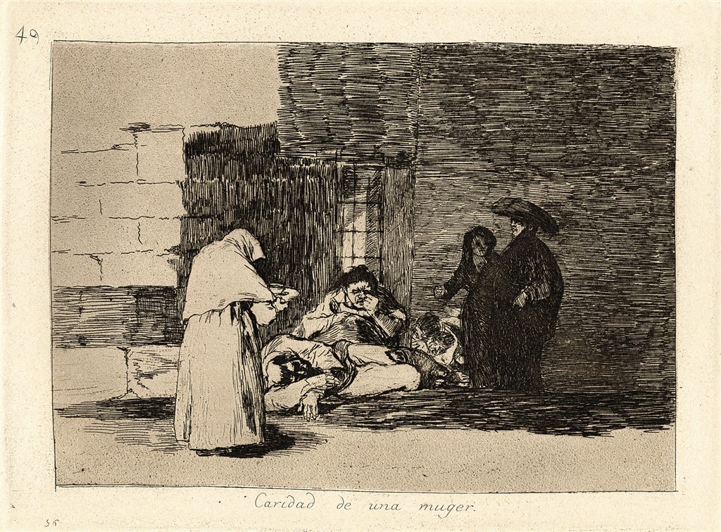
In the history of art, the “burin” was the tool used to cut lines. In modern tech, our burin is Extreme Ultraviolet (EUV) light. Traditional etching was limited by the physical size of the needle or the viscosity of the acid. Modern tech etching is limited by the wavelength of light itself.
By using EUV lithography, tech companies can etch patterns that are far smaller than the wavelength of visible light. This is where the “art” meets high-level physics. The machines that perform this etching are among the most expensive and complex tools ever created, costing hundreds of millions of dollars. They represent the pinnacle of human technical achievement, turning the concept of etching into a high-stakes race for computational power.
Digital Etching in Software and Creative Media
While the physical side of etching focuses on hardware, the “art of etching” also survives in the digital realm through software and user interface design. Software developers and digital artists use “etching” algorithms to simulate depth, texture, and permanence in digital environments.
Replicating Physicality: Algorithms and Texture Mapping
In digital art software like Adobe Photoshop or specialized 3D modeling tools like ZBrush, “etching” refers to the digital simulation of removing material. Through the use of height maps and normal maps, software can simulate the way light hits an “etched” surface in a virtual 3D space.
This is more than just a visual trick; it is an essential part of the “tech art” workflow in video game development and CGI. By using shaders that mimic the chemical “bite” of acid on metal, developers create immersive, realistic textures that give digital objects a sense of history and tangibility. This crossover shows that even as we move toward a purely digital existence, the aesthetic language of traditional etching remains vital to our visual technology.
Vector-Based Etching: The Art of Clean Lines in Modern UI/UX
In the world of UI/UX design, the concept of etching is applied to create “skeuomorphic” or “depth-aware” interfaces. When you see a button on a smartphone that looks like it is pressed into the screen, or a logo that appears “etched” into a digital header, you are seeing the technological application of intaglio principles.
Modern CSS and design frameworks use “inner shadows” and “drop shadows” to replicate the way an etched line holds shadow in the real world. This helps users understand the hierarchy and functionality of an interface. The “art” here lies in the subtle application of technology to make a flat glass screen feel like a tactile, three-dimensional tool.
The Future of Etching: Nanotechnology and Beyond
As we look toward the future, the technology of etching is moving into even more “artistic” and experimental territories. We are moving beyond 2D surfaces and into 3D nanostructures, where etching is used to build machines at the molecular level.
Molecular Manufacturing: The Ultimate Form of Precision Art
The next frontier of etching is “Atomic Layer Etching” (ALE). Unlike traditional chemical etching, which can be somewhat messy at a microscopic level, ALE allows engineers to remove material one single layer of atoms at a time. This is the ultimate expression of the etcher’s art—absolute control over matter.
This technology is being used to develop new types of sensors, medical devices that can travel through the bloodstream, and high-density memory storage. In this niche, the “artist” is the nanotechnologist, and the “art” is the creation of functional structures that are invisible to the naked eye but capable of changing the world.
Quantum Etching: Preparing for the Next Leap in Tech
As we enter the era of quantum computing, the etching process becomes even more critical. Quantum bits (qubits) are incredibly sensitive to their environment. Any imperfection in the etching of the superconducting circuits can lead to “noise” and cause the computer to fail.
The “art” of quantum etching involves creating perfectly smooth surfaces and junctions to preserve the quantum state. This requires a fusion of cryogenics, vacuum technology, and advanced chemistry. As we refine these techniques, the legacy of etching—starting from a simple scratch on a copper plate—will be what eventually unlocks the ability to solve the world’s most complex mathematical problems through quantum supremacy.
In conclusion, “etching in art” is no longer a term limited to the humanities. It is a vital technical descriptor for the processes that define our modern world. From the photolithography that powers our smartphones to the digital textures in our virtual worlds, the evolution of etching represents the perfect marriage of aesthetic vision and technological prowess. As we continue to shrink our tools and expand our digital capabilities, the art of the etch remains the most precise way we have to leave a permanent mark on the universe.
aViewFromTheCave is a participant in the Amazon Services LLC Associates Program, an affiliate advertising program designed to provide a means for sites to earn advertising fees by advertising and linking to Amazon.com. Amazon, the Amazon logo, AmazonSupply, and the AmazonSupply logo are trademarks of Amazon.com, Inc. or its affiliates. As an Amazon Associate we earn affiliate commissions from qualifying purchases.