
In the landscape of modern technology, we often marvel at the complexity of artificial intelligence, the sleek interface of a new smartphone, or the lightning-fast speeds of 5G networks. However, beneath the layers of high-level software and sophisticated user interfaces lies a fundamental physical reality: the movement of electrons. At the heart of every digital interaction and hardware innovation are conductors.
To understand the trajectory of technology—from the miniaturization of processors to the efficiency of electric vehicle (EV) batteries—one must first understand what conductors are, how they function, and how they are being re-engineered to meet the demands of the 21st century.

The Fundamental Physics of Conductivity
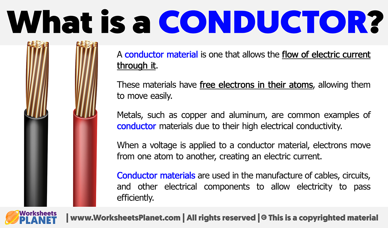
At its simplest, a conductor is a material that allows the flow of an electrical current. In the context of technology, this refers to the ease with which electrons move through a substance when a voltage is applied. This property is not accidental; it is a direct result of the atomic structure of the material.
The Atomic Level: Why Some Materials Flow
The behavior of a conductor is determined by its “valence electrons”—the electrons located in the outermost shell of an atom. In conductive materials, particularly metals, these valence electrons are not tightly bound to their parent nuclei. Instead, they form a “sea of electrons” that can drift freely through the material’s crystalline lattice.
When an external electric field is introduced, these free electrons move in a coordinated fashion, creating what we recognize as an electric current. This high “electron mobility” is the prerequisite for all electronic hardware. Without materials that exhibit this behavior, the transmission of data and power would be physically impossible.
Metals vs. Non-Metals: Identifying Efficient Paths
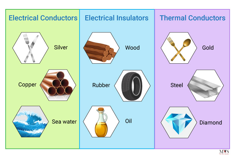
While many materials can carry a charge under extreme conditions, the tech industry relies on a specific hierarchy of conductors. Silver is technically the most conductive element, followed closely by copper and gold.
In tech manufacturing, copper is the industry standard for wiring and printed circuit boards (PCBs) due to its balance of high conductivity and cost-effectiveness. Gold, while expensive, is indispensable in high-end gadgets and digital security hardware because it does not corrode. When a smartphone manufacturer designs a connector or a high-performance relay, they choose gold to ensure a stable connection over years of use, preventing the signal degradation that would occur with oxidation.
From Copper to Superconductors: Types of Tech Conductors
As technology evolves, our reliance on standard copper wiring is being challenged by the need for faster data transmission and better energy efficiency. The tech sector is currently diversifying the types of conductors used in everything from consumer electronics to massive data centers.
Conventional Conductors: The Backbone of Hardware
Copper and aluminum remain the workhorses of the tech world. In your laptop, copper heat pipes and traces on the motherboard facilitate the movement of both power and information. Aluminum is frequently used in power distribution and the casings of devices like MacBooks, where it serves a dual purpose as a structural element and a thermal conductor to dissipate heat away from the internal chips.
The Breakthrough of Superconductivity
In the realm of high-performance computing (HPC) and quantum technology, standard conductors pose a problem: resistance. Resistance generates heat and leads to energy loss. Superconductors are materials that, when cooled to extremely low temperatures, exhibit zero electrical resistance.
This allows for the creation of incredibly powerful magnets and sensors. In quantum tech, superconductors are used to create “qubits,” the basic units of quantum information. Companies like IBM and Google are currently in a technological arms race to stabilize these superconducting states, as they hold the key to processing power that dwarfs today’s fastest supercomputers.
Graphene and Advanced Carbon Materials
One of the most exciting trends in tech materials is the rise of graphene. A single layer of carbon atoms arranged in a hexagonal lattice, graphene is significantly more conductive than copper. Its potential applications in tech are vast, ranging from flexible touchscreens to ultra-fast charging batteries and advanced electromagnetic shielding for digital security. Because it is incredibly thin and strong, it allows for the development of “wearable tech” that remains highly functional despite being subjected to constant physical stress.
Semiconductors: The Brains of the Digital Age
While conductors allow electricity to flow and insulators block it, the most important material in the modern tech stack is the semiconductor. Semiconductors are materials whose conductivity can be precisely controlled, acting as the “valves” of the digital world.
Silicon: The Essential Middle Ground
Silicon is the most famous semiconductor, lending its name to Silicon Valley. By itself, silicon is a mediocre conductor. However, its value lies in our ability to modify its properties. In a CPU or a GPU, billions of microscopic silicon switches (transistors) flip on and off to process binary code. The transition between “conducting” and “insulating” states is what allows a computer to perform logic operations.
Doping: How We Control Electron Flow
To turn silicon into a functional tech component, engineers use a process called “doping.” By adding minute amounts of impurities—like phosphorus or boron—into the silicon crystal, they can create an excess of electrons (N-type) or a deficit of electrons (P-type). The interaction between these two types of silicon at a junction is what enables the creation of transistors, diodes, and solar cells. This level of control is what separates modern “smart” tech from the simple electrical appliances of the past.
Wide Bandgap Materials (GaN and SiC)
A new trend in hardware is the shift toward Wide Bandgap (WBG) semiconductors, such as Gallium Nitride (GaN) and Silicon Carbide (SiC). These materials can handle much higher voltages and temperatures than traditional silicon. If you have purchased a high-speed “fast charger” for your phone recently, it likely uses GaN. This technology allows for smaller, more efficient power adapters that don’t overheat, representing a major leap in mobile tech convenience.
Engineering Challenges in High-Performance Tech
As we push the limits of what gadgets and AI tools can do, we encounter the physical limitations of our conductors. The “Tech” niche is currently defined by a struggle against physics—specifically, heat and scale.
Heat Management and Resistance
Whenever electricity flows through a conductor (that isn’t a superconductor), some energy is lost as heat. This is known as Joule heating. In data centers running massive AI models, heat is the enemy. It throttles performance and increases the risk of hardware failure. Modern tech reviews of laptops and GPUs often focus heavily on “thermal throttling,” which is essentially the device slowing down its conductors to prevent them from melting the internal components.
Miniaturization Limits and Moore’s Law
For decades, Moore’s Law—the observation that the number of transistors on a microchip doubles every two years—has driven tech progress. However, as we shrink conductors down to the nanometer scale, we run into the “quantum tunneling” effect. At this size, electrons can sometimes “jump” across insulators, leading to data errors and massive power leakage. Tech giants are currently researching “Extreme Ultraviolet Lithography” and new conductive materials to overcome these microscopic hurdles.
The Future: Conductors in Quantum and AI Computing
The next decade of technology will be defined by how we manipulate conductivity at the most granular levels. As AI tools demand more processing power, the physical infrastructure must evolve.
Enabling Next-Gen AI Hardware
AI-specific chips, like NVIDIA’s H100, require specialized conductive pathways to move massive amounts of data between memory and the processor at unprecedented speeds. We are seeing a move toward “optical interconnects”—using light (photons) instead of traditional metal conductors (electrons) for certain parts of the data journey. This hybrid approach promises to reduce latency and power consumption in the neural networks that power tools like ChatGPT and specialized AI software.
The Quest for Room-Temperature Superconductors
The “holy grail” of tech research is a room-temperature superconductor. If discovered and stabilized, it would revolutionize the world. We would have smartphones that never get hot, batteries that last for weeks, and a global power grid with zero energy loss. While recent headlines have shown both excitement and skepticism regarding various material claims (like LK-99), the tech industry’s focus remains laser-pointed on this frontier.
In conclusion, conductors are far more than just “wires.” They are the essential medium of the digital age. From the copper traces on a PCB to the silicon in a neural processing unit and the potential of graphene, conductors dictate the speed, efficiency, and capability of every piece of technology we use. As we continue to innovate in software and AI, our progress will ultimately be governed by our ability to master the materials that conduct the pulse of the digital world.
aViewFromTheCave is a participant in the Amazon Services LLC Associates Program, an affiliate advertising program designed to provide a means for sites to earn advertising fees by advertising and linking to Amazon.com. Amazon, the Amazon logo, AmazonSupply, and the AmazonSupply logo are trademarks of Amazon.com, Inc. or its affiliates. As an Amazon Associate we earn affiliate commissions from qualifying purchases.