
The modern world runs on silicon. From the data centers powering global artificial intelligence to the laptop used to write this article, the semiconductor is the fundamental building block of the digital age. At the center of this industry stands Intel, one of the few remaining companies that not only designs its own chips but also manufactures them. While many of its competitors, such as Apple, Nvidia, and AMD, operate as “fabless” entities—designing chips but outsourcing the actual physical production to third-party foundries like TSMC—Intel maintains a massive, multi-continental network of fabrication plants, known as “fabs.”

Understanding where Intel makes its chips is not just a matter of geography; it is a window into the most complex supply chain ever created by humanity. As geopolitical tensions rise and the demand for advanced computing power explodes, Intel’s manufacturing footprint has become a focal point of global tech strategy.
The Architecture of Global Production: Intel’s IDM 2.0 Strategy
To understand Intel’s manufacturing locations, one must first understand their operational philosophy: IDM 2.0. Historically, Intel was an Integrated Device Manufacturer (IDM), meaning they handled every step of the process in-house. Under the leadership of CEO Pat Gelsinger, the company evolved this into “IDM 2.0,” a three-pronged strategy that involves expanding internal factory capacity, utilizing third-party foundries when necessary, and, most importantly, launching Intel Foundry Services (IFS).
The Shift from Traditional Manufacturing to Foundry Services
For decades, Intel’s fabs were exclusive clubs, producing only Intel-branded processors. Today, the company is transforming its manufacturing sites into open-access hubs. This means that in the near future, a chip manufactured in an Intel plant in Arizona might actually be designed by a different tech giant. This shift has necessitated a massive investment in new facilities that can handle diverse architectures beyond Intel’s traditional x86 design.
Why Geographical Diversity Matters in Tech
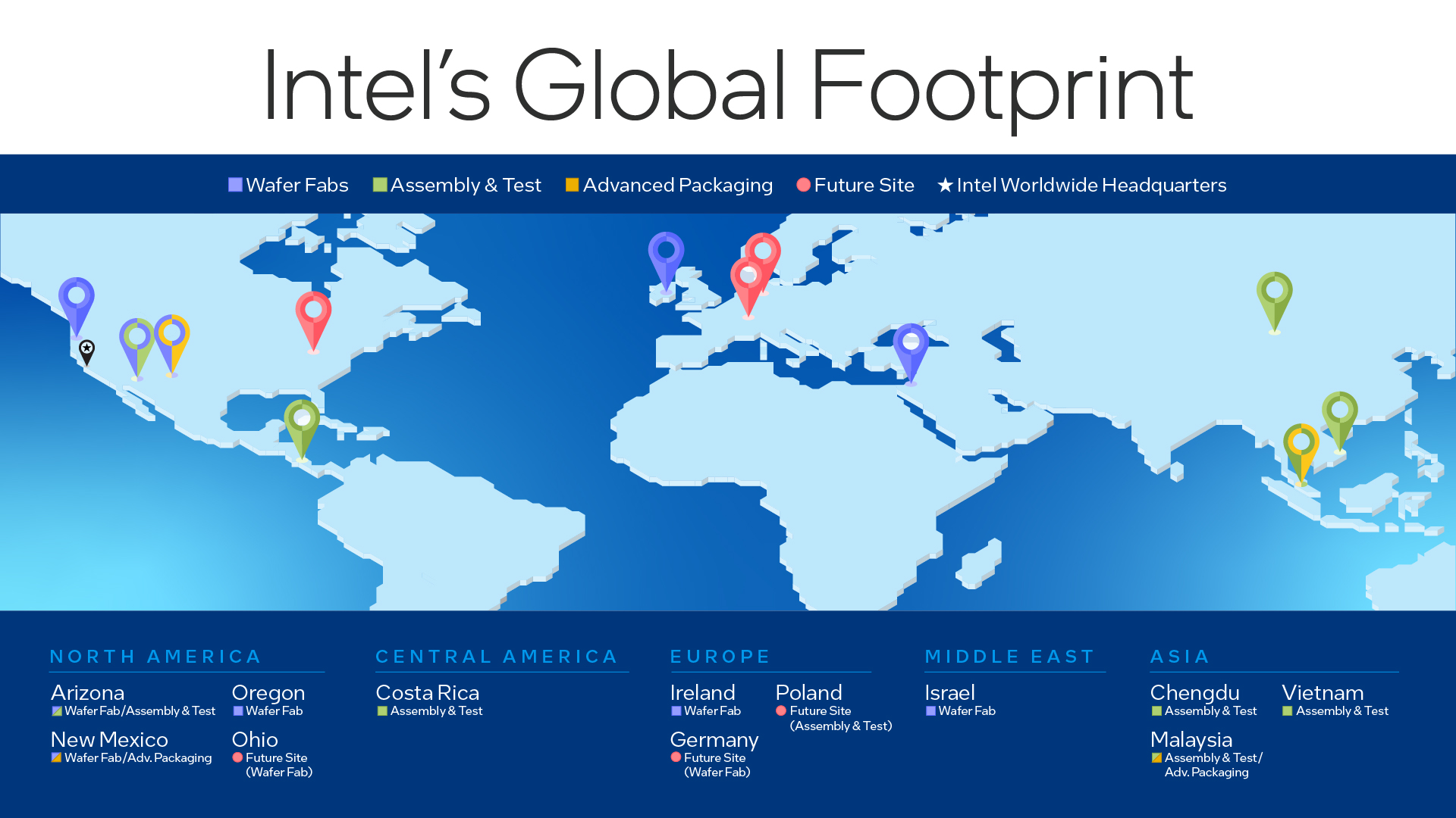
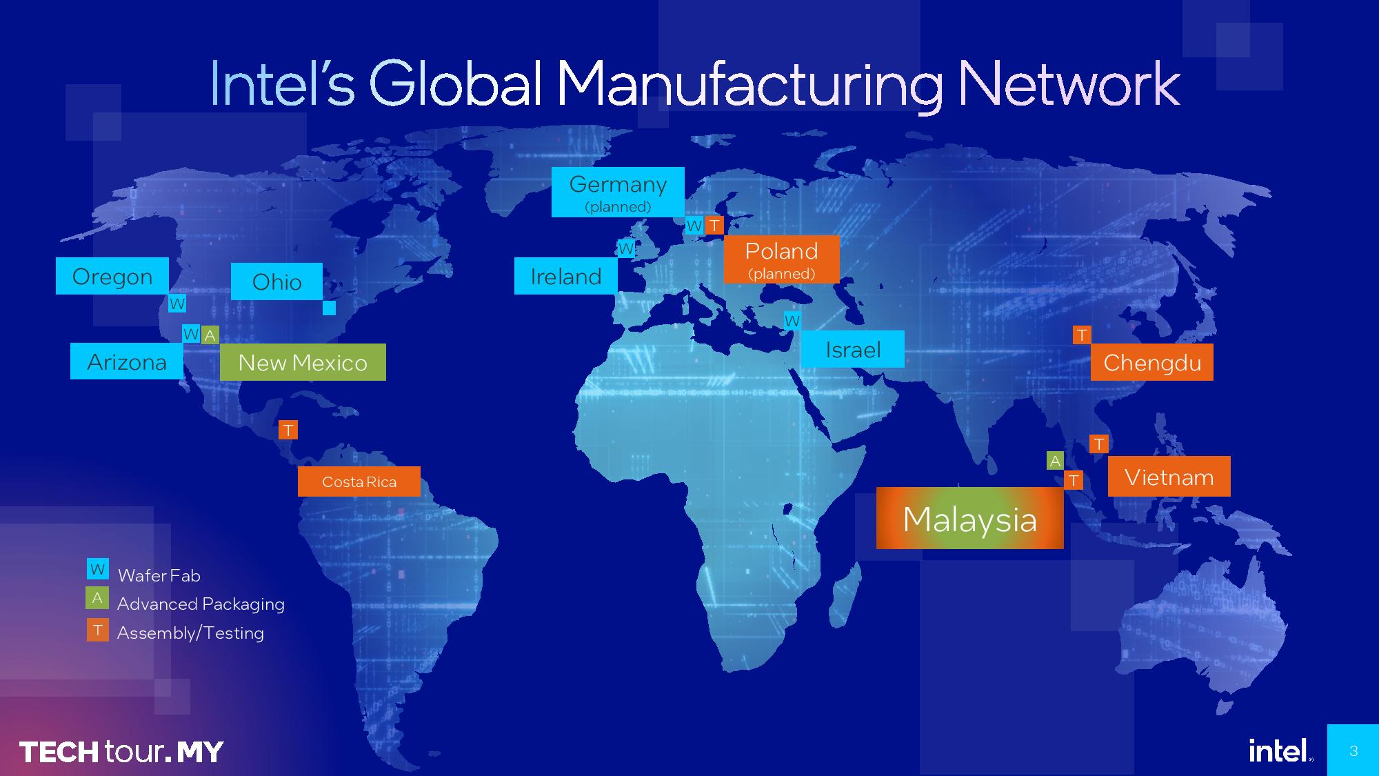
The semiconductor industry is notoriously sensitive to “single points of failure.” Natural disasters, regional instability, or trade disputes can halt global tech production overnight. Intel has countered this risk by spreading its manufacturing across three primary regions: North America, Europe, and Asia. This “balanced” supply chain ensures that the company can continue to produce leading-edge nodes (the technical term for generations of chip technology) even if one region faces disruption.
Domestic Powerhouse: Intel’s Footprint in the United States
The United States remains the primary engine for Intel’s research, development, and high-volume manufacturing. As the U.S. government pushes for “reshoring” critical technology through the CHIPS and Science Act, Intel’s domestic facilities are undergoing a historic expansion.
Oregon: The Heart of Research and Development
The Gordon Moore Park at Ronler Acres in Hillsboro, Oregon, is arguably the most advanced tech facility on the planet. This site serves as the “mother fab”—the place where Intel develops new process technologies before they are exported to other factories worldwide.
In Oregon, engineers work on the bleeding edge of lithography. This is where Intel first deployed Extreme Ultraviolet (EUV) lithography at scale. Because research and manufacturing happen in the same location, Intel can troubleshoot the transition from a laboratory setting to mass production with unprecedented speed. Every new generation of Intel Core or Xeon processors begins its life in the “Silicon Forest” of Oregon.
Arizona and New Mexico: Scaling for the Future
If Oregon is the brain of the operation, Arizona is the muscle. The Ocotillo campus in Chandler, Arizona, is Intel’s largest domestic manufacturing site. With several massive fabs currently in operation and two brand-new facilities (Fab 52 and Fab 62) under construction, Arizona is becoming a global epicenter for semiconductor high-volume manufacturing.
Meanwhile, in Rio Rancho, New Mexico, Intel focuses on the “back-end” of the process: packaging. As transistors approach the physical limits of atomic scale, how chips are stacked and connected—known as “advanced packaging”—becomes just as important as the chips themselves. The New Mexico site is home to Foveros, Intel’s breakthrough 3D packaging technology that allows different “chiplets” to be stacked vertically.
The Ohio “Mega-Site” and the CHIPS Act
Perhaps the most ambitious project in Intel’s history is the new site in Licking County, Ohio. Intel has committed an initial $20 billion to build two leading-edge fabs on a nearly 1,000-acre site. This “Mega-Site” is designed to eventually house up to eight fabs. This project represents a shift in the tech landscape, moving the center of gravity for American chipmaking into the Midwest and creating a new “Silicon Heartland.”
European Expansion: Strengthening the Continental Supply Chain
Europe has emerged as a vital pillar of Intel’s global strategy. With the European Union seeking to double its share of global semiconductor production by 2030, Intel is investing tens of billions of euros to expand its presence on the continent.
Ireland: The European Manufacturing Hub
For over 30 years, Leixlip, Ireland, has been the home of Intel’s European operations. The Fab 34 facility in Ireland recently made headlines for being the first in Europe to use EUV technology in high-volume manufacturing. This site produces the “Intel 4” process node, which powers the latest generation of energy-efficient laptops and AI-ready PCs. The Irish facility is a masterclass in modern tech logistics, receiving raw silicon wafers and transforming them into finished processors that supply markets across Europe, the Middle East, and Africa.
Germany and Poland: The Next Frontier of Silicon
Intel’s future in Europe is anchored in Germany and Poland. In Magdeburg, Germany, Intel is planning a massive “Silicon Junction” manufacturing complex. This facility is intended to deliver chips using the most advanced “Angstrom-era” nodes (such as Intel 18A), serving both Intel’s needs and those of external foundry customers.
To support this manufacturing, Intel is also building a new Semiconductor Assembly and Test facility in Wrocław, Poland. By placing assembly and testing in close proximity to the German fabs, Intel creates an end-to-end European ecosystem that reduces the reliance on shipping components back and forth to Asia.
Asian Operations: Assembly, Testing, and Regional Logistics
While most of the “front-end” fabrication (the actual printing of circuits on silicon wafers) happens in the US, Ireland, and Israel, the “back-end” of the process is heavily concentrated in Asia.
Vietnam and Malaysia: The Back-End Crucial to Success
Intel’s facilities in Ho Chi Minh City, Vietnam, and Kulim and Penang, Malaysia, are essential for the final stages of a chip’s journey. Once a wafer is printed in Oregon or Arizona, it is shipped to these Asian facilities. Here, the wafers are sliced into individual “dies,” tested for defects, and placed into the protective packages that allow them to be soldered onto motherboards.
Malaysia, in particular, is undergoing a massive upgrade. Intel is building its first overseas facility for advanced 3D packaging in Penang. This indicates a shift in the Asian role—moving from simple assembly to highly complex, tech-intensive manufacturing processes.
Israel: A Global Center for Innovation and Production
Intel Israel is a powerhouse of both design and manufacturing. The Kiryat Gat site operates some of Intel’s most productive fabs. Many of the most successful processor architectures in Intel’s history, including the “Centrino” mobile platform and several generations of Core processors, were designed and produced in Israel. Intel is currently expanding its Israeli footprint with Fab 38, a multibillion-dollar project that reinforces the country’s role as a critical node in the global tech supply chain.
The Future of Chipmaking: Leading-Edge Nodes and Sustainability
As Intel moves toward its goal of “five nodes in four years,” the technical complexity of these manufacturing sites is increasing exponentially. The transition from “Intel 7” to “Intel 18A” represents a leap in transistor density that requires a complete overhaul of factory equipment.
The Push Toward 18A and Beyond
The “A” in 18A stands for Angstrom, a unit of measurement smaller than a nanometer. To manufacture at this scale, Intel’s fabs are being equipped with High-NA (Numerical Aperture) EUV machines. These machines, produced by the Dutch company ASML, are the size of a double-decker bus and cost over $350 million each. Intel was the first in the industry to take delivery of these machines, placing them in the Oregon development site. This technology allows for even finer circuit patterns, enabling the AI chips of the 2026–2030 era.
Environmental Impact and Circular Tech Economy
Manufacturing chips is a resource-intensive process requiring massive amounts of electricity and ultra-pure water. As Intel expands its global footprint, it has committed to “net-positive” water use and 100% renewable electricity across its global operations by 2030. In locations like Arizona, where water is a scarce resource, Intel has implemented advanced circular water systems that treat and return nearly all the water used in the manufacturing process back to the local community.
The question of “where” Intel makes its chips is answered by a map that spans from the deserts of the American Southwest to the tech corridors of Europe and the bustling industrial zones of Southeast Asia. Each site plays a specialized role in a process that transforms common sand into the most complex devices ever built. By diversifying its manufacturing across the globe, Intel is not just building chips; it is building the infrastructure that will define the next decade of technological progress.
aViewFromTheCave is a participant in the Amazon Services LLC Associates Program, an affiliate advertising program designed to provide a means for sites to earn advertising fees by advertising and linking to Amazon.com. Amazon, the Amazon logo, AmazonSupply, and the AmazonSupply logo are trademarks of Amazon.com, Inc. or its affiliates. As an Amazon Associate we earn affiliate commissions from qualifying purchases.